| Article ID | Journal | Published Year | Pages | File Type |
|---|---|---|---|---|
| 10411701 | Solid-State Electronics | 2005 | 16 Pages |
Abstract
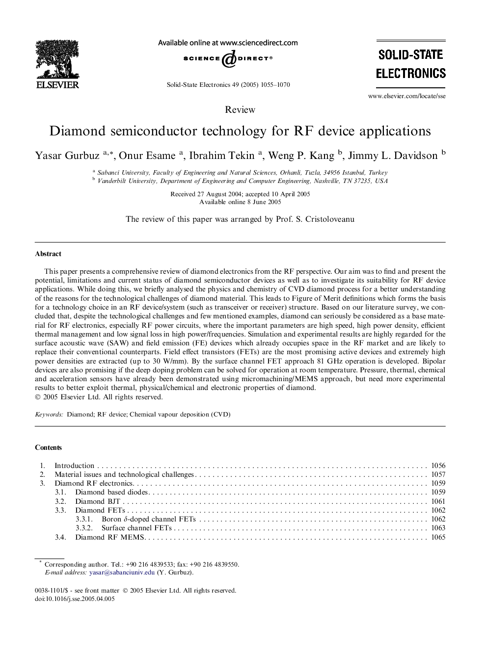
This paper presents a comprehensive review of diamond electronics from the RF perspective. Our aim was to find and present the potential, limitations and current status of diamond semiconductor devices as well as to investigate its suitability for RF device applications. While doing this, we briefly analysed the physics and chemistry of CVD diamond process for a better understanding of the reasons for the technological challenges of diamond material. This leads to Figure of Merit definitions which forms the basis for a technology choice in an RF device/system (such as transceiver or receiver) structure. Based on our literature survey, we concluded that, despite the technological challenges and few mentioned examples, diamond can seriously be considered as a base material for RF electronics, especially RF power circuits, where the important parameters are high speed, high power density, efficient thermal management and low signal loss in high power/frequencies. Simulation and experimental results are highly regarded for the surface acoustic wave (SAW) and field emission (FE) devices which already occupies space in the RF market and are likely to replace their conventional counterparts. Field effect transistors (FETs) are the most promising active devices and extremely high power densities are extracted (up to 30 W/mm). By the surface channel FET approach 81 GHz operation is developed. Bipolar devices are also promising if the deep doping problem can be solved for operation at room temperature. Pressure, thermal, chemical and acceleration sensors have already been demonstrated using micromachining/MEMS approach, but need more experimental results to better exploit thermal, physical/chemical and electronic properties of diamond.
Related Topics
Physical Sciences and Engineering
Engineering
Electrical and Electronic Engineering
Authors
Yasar Gurbuz, Onur Esame, Ibrahim Tekin, Weng P. Kang, Jimmy L. Davidson,
