| Article ID | Journal | Published Year | Pages | File Type |
|---|---|---|---|---|
| 1544186 | Physica E: Low-dimensional Systems and Nanostructures | 2015 | 6 Pages |
•SiO2 nanowires are produced directly on a Si surface.•The SiO2 nanowires are coated by Au films.•The Au films are transformed in nanoparticles by thermal-induced dewetting processes.•The activation energy for the dewetting process of Au films on SiO2 nanowires is evaluated.
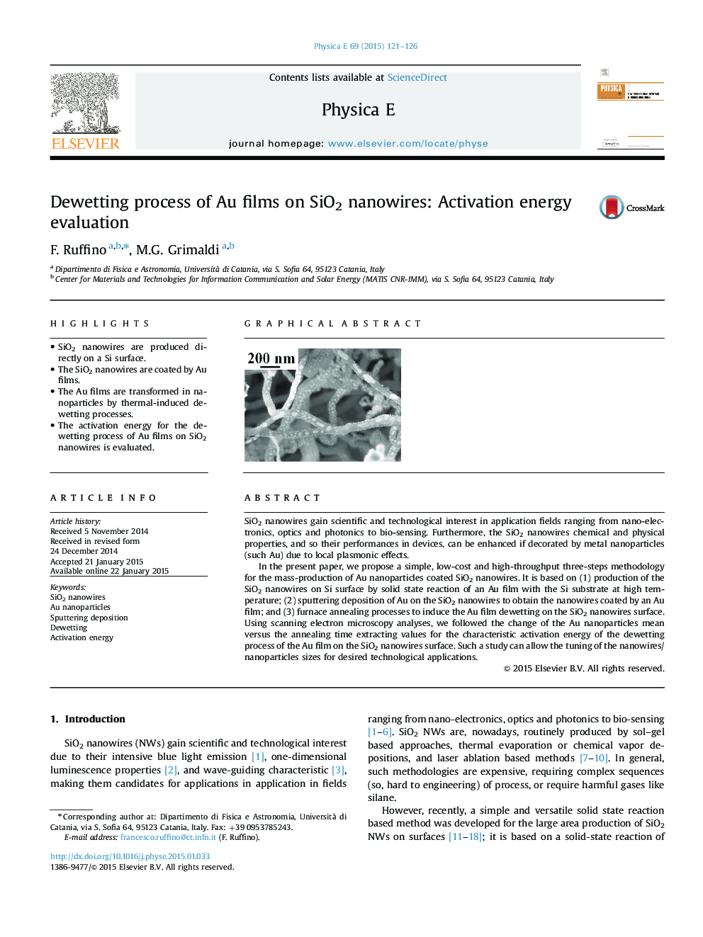
SiO2 nanowires gain scientific and technological interest in application fields ranging from nano-electronics, optics and photonics to bio-sensing. Furthermore, the SiO2 nanowires chemical and physical properties, and so their performances in devices, can be enhanced if decorated by metal nanoparticles (such Au) due to local plasmonic effects.In the present paper, we propose a simple, low-cost and high-throughput three-steps methodology for the mass-production of Au nanoparticles coated SiO2 nanowires. It is based on (1) production of the SiO2 nanowires on Si surface by solid state reaction of an Au film with the Si substrate at high temperature; (2) sputtering deposition of Au on the SiO2 nanowires to obtain the nanowires coated by an Au film; and (3) furnace annealing processes to induce the Au film dewetting on the SiO2 nanowires surface. Using scanning electron microscopy analyses, we followed the change of the Au nanoparticles mean versus the annealing time extracting values for the characteristic activation energy of the dewetting process of the Au film on the SiO2 nanowires surface. Such a study can allow the tuning of the nanowires/nanoparticles sizes for desired technological applications.
Graphical abstractFigure optionsDownload full-size imageDownload as PowerPoint slide
