| Article ID | Journal | Published Year | Pages | File Type |
|---|---|---|---|---|
| 1590815 | Science and Technology of Advanced Materials | 2007 | 5 Pages |
Abstract
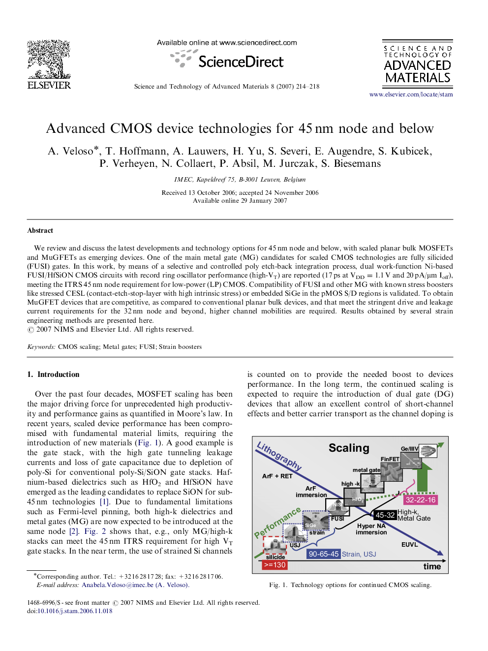
We review and discuss the latest developments and technology options for 45 nm node and below, with scaled planar bulk MOSFETs and MuGFETs as emerging devices. One of the main metal gate (MG) candidates for scaled CMOS technologies are fully silicided (FUSI) gates. In this work, by means of a selective and controlled poly etch-back integration process, dual work-function Ni-based FUSI/HfSiON CMOS circuits with record ring oscillator performance (high-VT) are reported (17 ps at VDD=1.1 V and 20 pA/μm Ioff), meeting the ITRS 45 nm node requirement for low-power (LP) CMOS. Compatibility of FUSI and other MG with known stress boosters like stressed CESL (contact-etch-stop-layer with high intrinsic stress) or embedded SiGe in the pMOS S/D regions is validated. To obtain MuGFET devices that are competitive, as compared to conventional planar bulk devices, and that meet the stringent drive and leakage current requirements for the 32 nm node and beyond, higher channel mobilities are required. Results obtained by several strain engineering methods are presented here.
Keywords
Related Topics
Physical Sciences and Engineering
Materials Science
Materials Science (General)
Authors
A. Veloso, T. Hoffmann, A. Lauwers, H. Yu, S. Severi, E. Augendre, S. Kubicek, P. Verheyen, N. Collaert, P. Absil, M. Jurczak, S. Biesemans,
