| Article ID | Journal | Published Year | Pages | File Type |
|---|---|---|---|---|
| 1648235 | Materials Letters | 2011 | 4 Pages |
Abstract
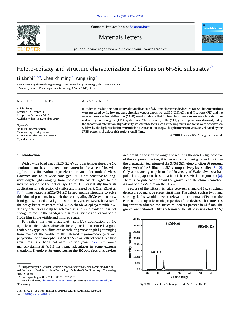
In order to realize the non-ultraviolet application of SiC optoelectronic devices, Si/6H-SiC heterojunctions were prepared by the low-pressure chemical vapour deposition at 850 °C. The X-ray diffraction (XRD) and the selected area electron diffraction (SAED) results indicate that Si thin films have a monocrystalline structure and were grown along the (111) crystal plane. The rationality of the (111) growth plane was also analyzed by the theoretical calculation. High-density structural defects such as stacking faults and twins were observed on Si films by the high-resolution transmission electron microscopy. This phenomenon was also validated by the SAED patterns of defect-rich regions on Si films.
Related Topics
Physical Sciences and Engineering
Materials Science
Nanotechnology
Authors
Li Lianbi, Chen Zhiming, Yang Ying,
