| Article ID | Journal | Published Year | Pages | File Type |
|---|---|---|---|---|
| 1674869 | Thin Solid Films | 2005 | 4 Pages |
Abstract
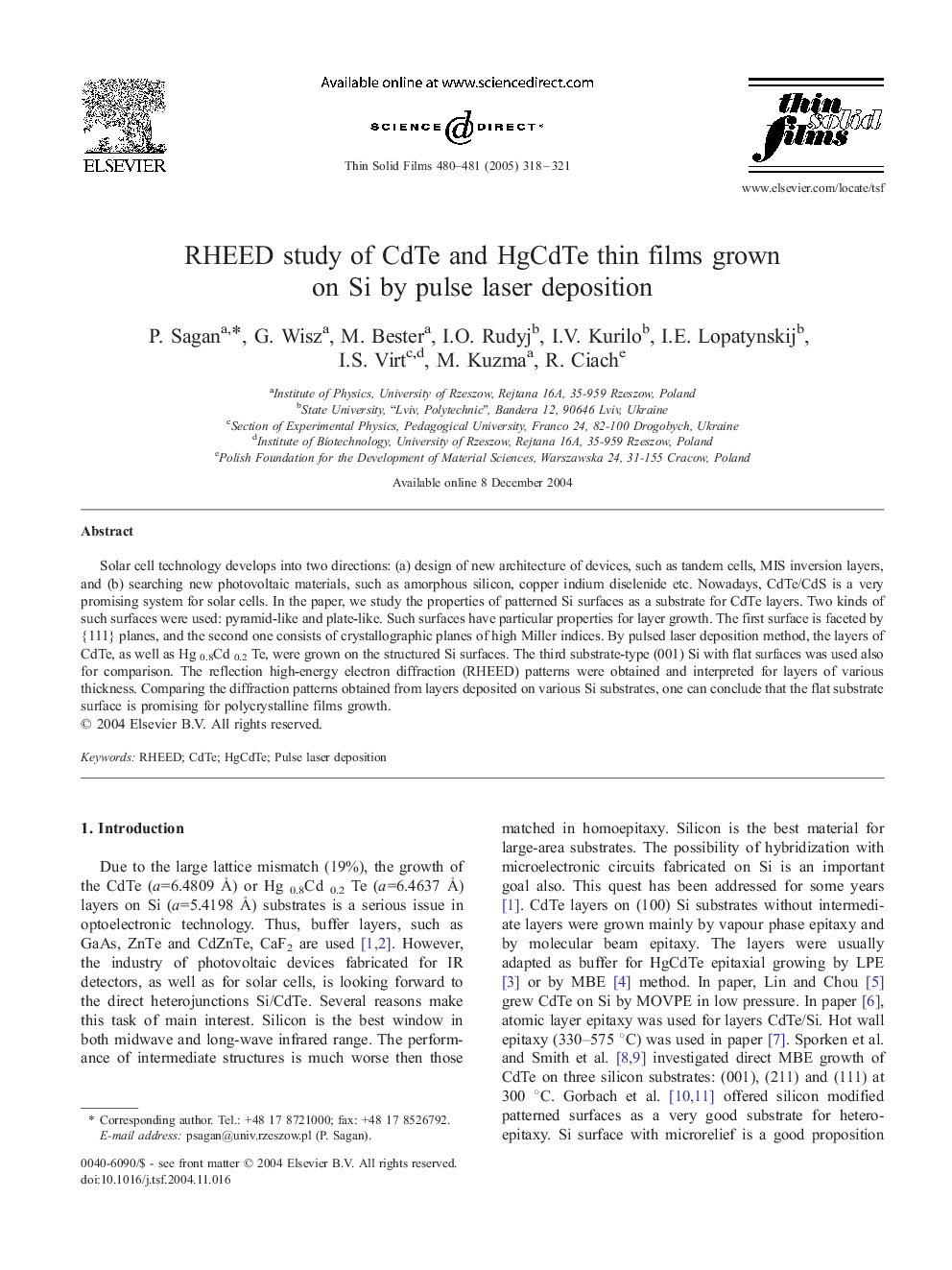
Solar cell technology develops into two directions: (a) design of new architecture of devices, such as tandem cells, MIS inversion layers, and (b) searching new photovoltaic materials, such as amorphous silicon, copper indium diselenide etc. Nowadays, CdTe/CdS is a very promising system for solar cells. In the paper, we study the properties of patterned Si surfaces as a substrate for CdTe layers. Two kinds of such surfaces were used: pyramid-like and plate-like. Such surfaces have particular properties for layer growth. The first surface is faceted by {111} planes, and the second one consists of crystallographic planes of high Miller indices. By pulsed laser deposition method, the layers of CdTe, as well as Hg 0.8Cd 0.2 Te, were grown on the structured Si surfaces. The third substrate-type (001) Si with flat surfaces was used also for comparison. The reflection high-energy electron diffraction (RHEED) patterns were obtained and interpreted for layers of various thickness. Comparing the diffraction patterns obtained from layers deposited on various Si substrates, one can conclude that the flat substrate surface is promising for polycrystalline films growth.
Related Topics
Physical Sciences and Engineering
Materials Science
Nanotechnology
Authors
P. Sagan, G. Wisz, M. Bester, I.O. Rudyj, I.V. Kurilo, I.E. Lopatynskij, I.S. Virt, M. Kuzma, R. Ciach,
