| Article ID | Journal | Published Year | Pages | File Type |
|---|---|---|---|---|
| 1676293 | Thin Solid Films | 2007 | 5 Pages |
Abstract
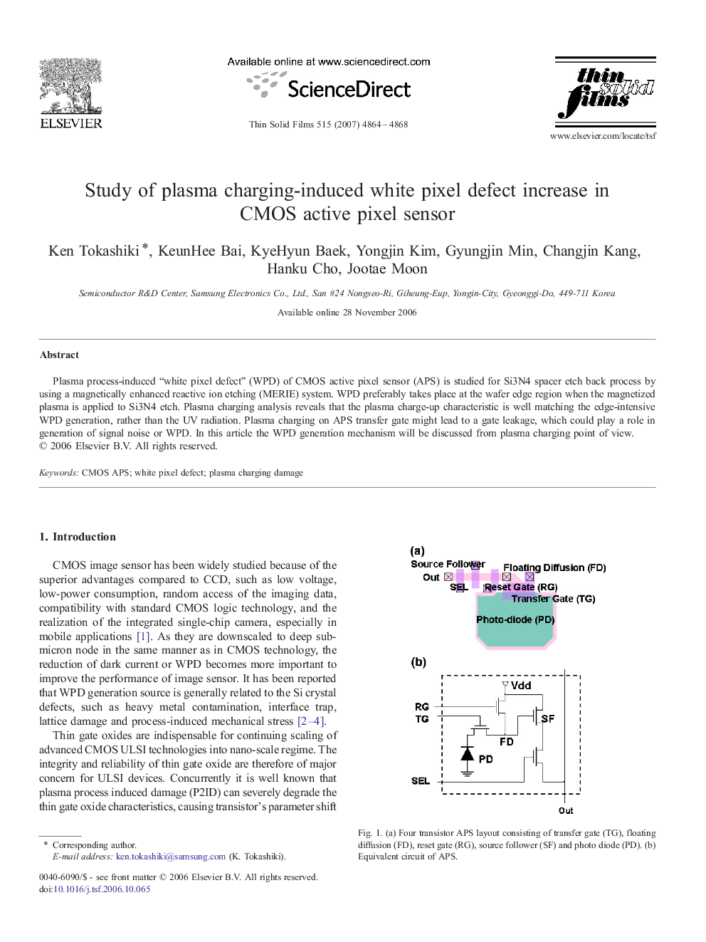
Plasma process-induced “white pixel defect” (WPD) of CMOS active pixel sensor (APS) is studied for Si3N4 spacer etch back process by using a magnetically enhanced reactive ion etching (MERIE) system. WPD preferably takes place at the wafer edge region when the magnetized plasma is applied to Si3N4 etch. Plasma charging analysis reveals that the plasma charge-up characteristic is well matching the edge-intensive WPD generation, rather than the UV radiation. Plasma charging on APS transfer gate might lead to a gate leakage, which could play a role in generation of signal noise or WPD. In this article the WPD generation mechanism will be discussed from plasma charging point of view.
Keywords
Related Topics
Physical Sciences and Engineering
Materials Science
Nanotechnology
Authors
Ken Tokashiki, KeunHee Bai, KyeHyun Baek, Yongjin Kim, Gyungjin Min, Changjin Kang, Hanku Cho, Jootae Moon,
