| Article ID | Journal | Published Year | Pages | File Type |
|---|---|---|---|---|
| 5023763 | Materials & Design | 2017 | 11 Pages |
â¢A novel highly scalable multi-laser powder bed additive manufacturing approach for processing metallic alloys.â¢Near full melting of stainless steel alloy powder (99.7% density) using customised low power diode emitters (2.63 W).â¢Increased laser absorption and reduced laser power requirement through use of shorter laser wavelength.
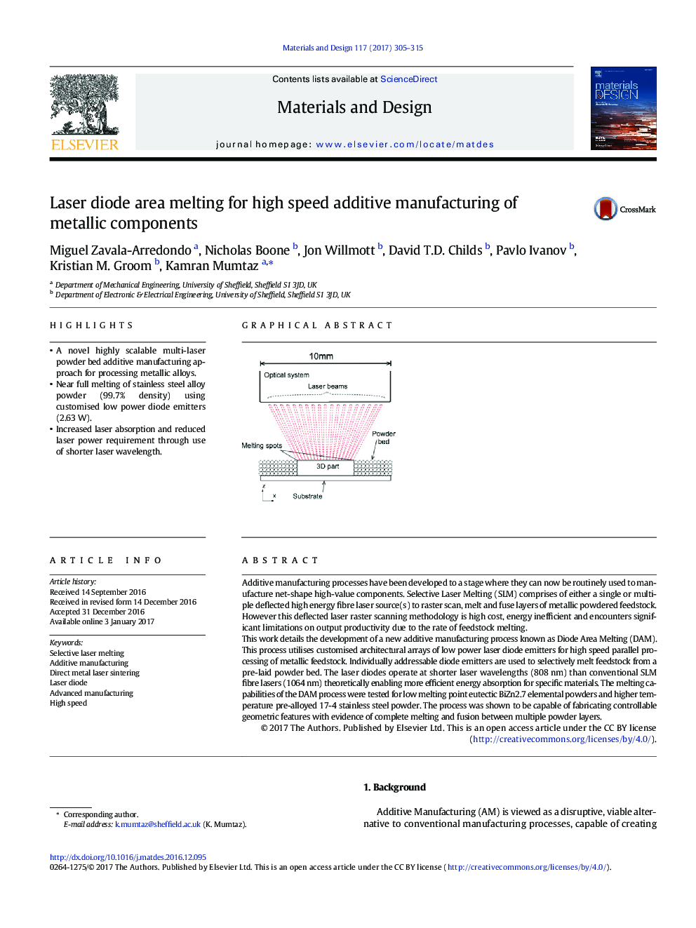
Additive manufacturing processes have been developed to a stage where they can now be routinely used to manufacture net-shape high-value components. Selective Laser Melting (SLM) comprises of either a single or multiple deflected high energy fibre laser source(s) to raster scan, melt and fuse layers of metallic powdered feedstock. However this deflected laser raster scanning methodology is high cost, energy inefficient and encounters significant limitations on output productivity due to the rate of feedstock melting.This work details the development of a new additive manufacturing process known as Diode Area Melting (DAM). This process utilises customised architectural arrays of low power laser diode emitters for high speed parallel processing of metallic feedstock. Individually addressable diode emitters are used to selectively melt feedstock from a pre-laid powder bed. The laser diodes operate at shorter laser wavelengths (808Â nm) than conventional SLM fibre lasers (1064Â nm) theoretically enabling more efficient energy absorption for specific materials. The melting capabilities of the DAM process were tested for low melting point eutectic BiZn2.7 elemental powders and higher temperature pre-alloyed 17-4 stainless steel powder. The process was shown to be capable of fabricating controllable geometric features with evidence of complete melting and fusion between multiple powder layers.
Graphical abstractDownload high-res image (84KB)Download full-size image
