| Article ID | Journal | Published Year | Pages | File Type |
|---|---|---|---|---|
| 7119793 | Materials Science in Semiconductor Processing | 2014 | 6 Pages |
Abstract
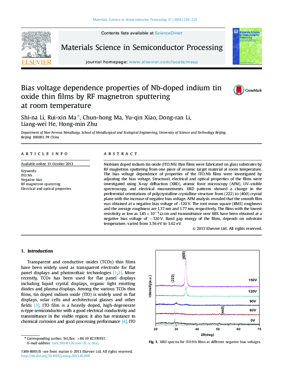
Niobium doped indium tin oxide (ITO:Nb) thin films were fabricated on glass substrates by RF magnetron sputtering from one piece of ceramic target material at room temperature. The bias voltage dependence of properties of the ITO:Nb films were investigated by adjusting the bias voltage. Structural, electrical and optical properties of the films were investigated using X-ray diffraction (XRD), atomic force microscopy (AFM), UV-visible spectroscopy, and electrical measurements. XRD patterns showed a change in the preferential orientations of polycrystalline crystalline structure from (222) to (400) crystal plane with the increase of negative bias voltage. AFM analysis revealed that the smooth film was obtained at a negative bias voltage of -120 V. The root mean square (RMS) roughness and the average roughness are 1.37 nm and 1.77 nm, respectively. The films with the lowest resistivity as low as 1.45Ã10â4 Ω cm and transmittance over 88% have been obtained at a negative bias voltage of â120 V. Band gap energy of the films, depends on substrate temperature, varied from 3.56 eV to 3.62 eV.
Related Topics
Physical Sciences and Engineering
Engineering
Electrical and Electronic Engineering
Authors
Shi-na Li, Rui-xin Ma, Chun-hong Ma, Yu-qin Xiao, Dong-ran Li, Liang-wei He, Hong-min Zhu,
