| Article ID | Journal | Published Year | Pages | File Type |
|---|---|---|---|---|
| 9618657 | Solar Energy Materials and Solar Cells | 2005 | 8 Pages |
Abstract
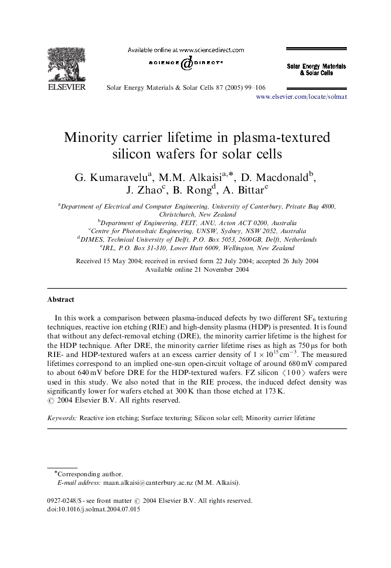
In this work a comparison between plasma-induced defects by two different SF6 texturing techniques, reactive ion etching (RIE) and high-density plasma (HDP) is presented. It is found that without any defect-removal etching (DRE), the minority carrier lifetime is the highest for the HDP technique. After DRE, the minority carrier lifetime rises as high as 750 μs for both RIE- and HDP-textured wafers at an excess carrier density of 1Ã1015 cmâ3. The measured lifetimes correspond to an implied one-sun open-circuit voltage of around 680 mV compared to about 640 mV before DRE for the HDP-textured wafers. FZ silicon ã1 0 0ã wafers were used in this study. We also noted that in the RIE process, the induced defect density was significantly lower for wafers etched at 300 K than those etched at 173 K.
Related Topics
Physical Sciences and Engineering
Chemical Engineering
Catalysis
Authors
G. Kumaravelu, M.M. Alkaisi, D. Macdonald, J. Zhao, B. Rong, A. Bittar,
