| Article ID | Journal | Published Year | Pages | File Type |
|---|---|---|---|---|
| 9809448 | Surface and Coatings Technology | 2005 | 4 Pages |
Abstract
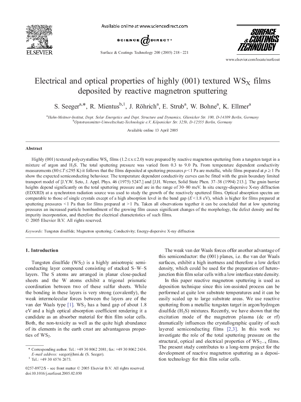
Highly (001) textured polycrystalline WSx films (1.2 â¤Â x â¤Â 2.0) were prepared by reactive magnetron sputtering from a tungsten target in a mixture of argon and H2S. The total sputtering pressure was varied from 0.3 to 9.0 Pa. From temperature dependent conductivity measurements (80 â¤Â T â¤Â 295 K) it follows that the films deposited at sputtering pressures p < 1 Pa are metallic, while films prepared at p â¥Â 1 Pa show the expected semiconducting behaviour. The temperature dependent conductivity curves can be fitted with the grain boundary limited transport model of [J.Y.W. Seto, J. Appl. Phys. 46 (1975) 5247.] and [J.H. Werner, Solid State Phen. 37-38 (1994) 213.]. The grain barrier heights depend significantly on the total sputtering pressure and are in the range of 30-80 meV. In situ energy-dispersive X-ray diffraction (EDXRD) at a synchrotron radiation source was used to study the growth of the reactively sputtered films. Optical absorption spectra are comparable to those of single crystals except of a high absorption level in the band gap (E < 1.8 eV), which is higher for films prepared at sputtering pressures < 1 Pa than for films prepared at > 1 Pa. Taken all observations together it can be concluded that at low sputtering pressures an increased particle bombardment of the growing film causes significant changes of the morphology, the defect density and the impurity incorporation, and therefore the electrical characteristics of such films.
Related Topics
Physical Sciences and Engineering
Materials Science
Nanotechnology
Authors
S. Seeger, R. Mientus, J. Röhrich, E. Strub, W. Bohne, K. Ellmer,
