| Article ID | Journal | Published Year | Pages | File Type |
|---|---|---|---|---|
| 9830315 | Journal of Crystal Growth | 2005 | 5 Pages |
Abstract
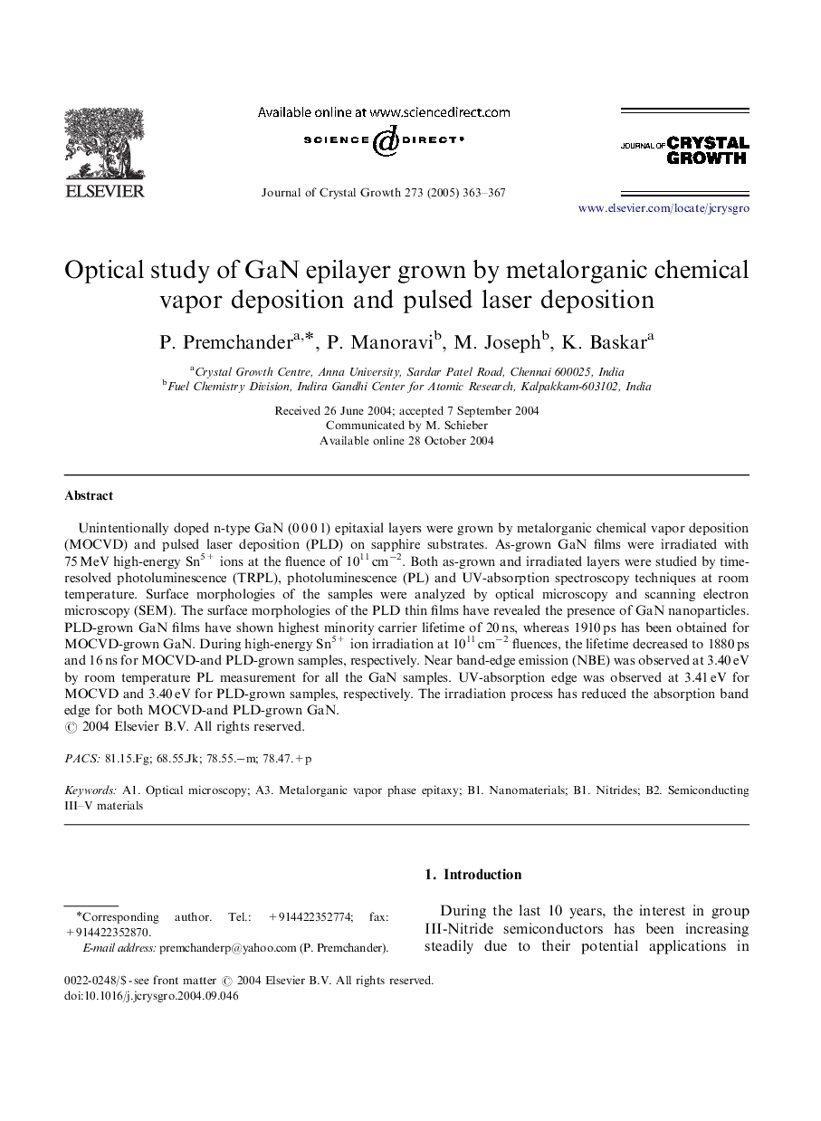
Unintentionally doped n-type GaN (0Â 0Â 0Â 1) epitaxial layers were grown by metalorganic chemical vapor deposition (MOCVD) and pulsed laser deposition (PLD) on sapphire substrates. As-grown GaN films were irradiated with 75Â MeV high-energy Sn5+ ions at the fluence of 1011Â cmâ2. Both as-grown and irradiated layers were studied by time-resolved photoluminescence (TRPL), photoluminescence (PL) and UV-absorption spectroscopy techniques at room temperature. Surface morphologies of the samples were analyzed by optical microscopy and scanning electron microscopy (SEM). The surface morphologies of the PLD thin films have revealed the presence of GaN nanoparticles. PLD-grown GaN films have shown highest minority carrier lifetime of 20Â ns, whereas 1910Â ps has been obtained for MOCVD-grown GaN. During high-energy Sn5+ ion irradiation at 1011Â cmâ2 fluences, the lifetime decreased to 1880Â ps and 16Â ns for MOCVD-and PLD-grown samples, respectively. Near band-edge emission (NBE) was observed at 3.40Â eV by room temperature PL measurement for all the GaN samples. UV-absorption edge was observed at 3.41Â eV for MOCVD and 3.40Â eV for PLD-grown samples, respectively. The irradiation process has reduced the absorption band edge for both MOCVD-and PLD-grown GaN.
Keywords
Related Topics
Physical Sciences and Engineering
Physics and Astronomy
Condensed Matter Physics
Authors
P. Premchander, P. Manoravi, M. Joseph, K. Baskar,
