| Article ID | Journal | Published Year | Pages | File Type |
|---|---|---|---|---|
| 5454398 | Journal of Nuclear Materials | 2016 | 8 Pages |
â¢In situ TEM He+ implantation and annealing was performed on nanocrystalline iron.â¢Small grains limited loop size and resulted in complete disappearance of loops by 600 °C.â¢Implantation followed by annealing resulted in cavities evenly distributed through grain.â¢Cavities predominately observed at grain boundaries after He+ implantation at 600 °C.
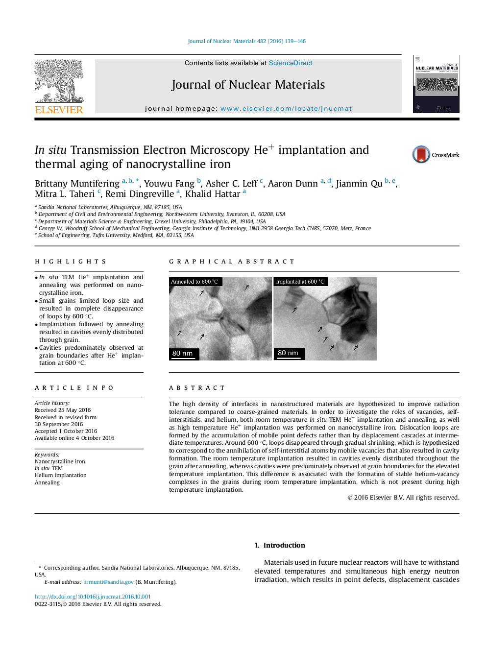
The high density of interfaces in nanostructured materials are hypothesized to improve radiation tolerance compared to coarse-grained materials. In order to investigate the roles of vacancies, self-interstitials, and helium, both room temperature in situ TEM He+ implantation and annealing, as well as high temperature He+ implantation was performed on nanocrystalline iron. Dislocation loops are formed by the accumulation of mobile point defects rather than by displacement cascades at intermediate temperatures. Around 600 °C, loops disappeared through gradual shrinking, which is hypothesized to correspond to the annihilation of self-interstitial atoms by mobile vacancies that also resulted in cavity formation. The room temperature implantation resulted in cavities evenly distributed throughout the grain after annealing, whereas cavities were predominately observed at grain boundaries for the elevated temperature implantation. This difference is associated with the formation of stable helium-vacancy complexes in the grains during room temperature implantation, which is not present during high temperature implantation.
Graphical abstractDownload high-res image (200KB)Download full-size image
