| Article ID | Journal | Published Year | Pages | File Type |
|---|---|---|---|---|
| 10364190 | Microelectronic Engineering | 2005 | 7 Pages |
Abstract
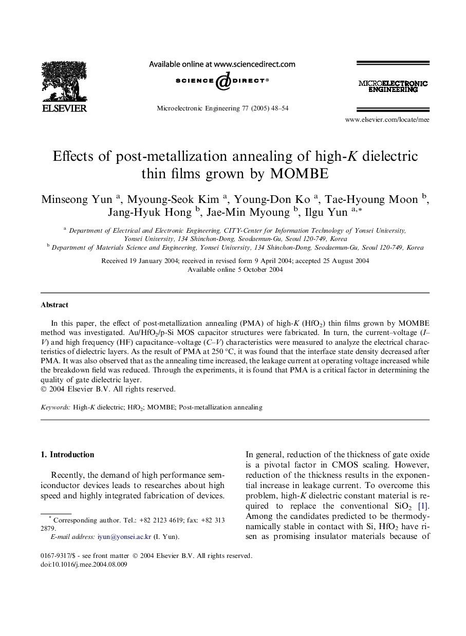
In this paper, the effect of post-metallization annealing (PMA) of high-K (HfO2) thin films grown by MOMBE method was investigated. Au/HfO2/p-Si MOS capacitor structures were fabricated. In turn, the current-voltage (I-V) and high frequency (HF) capacitance-voltage (C-V) characteristics were measured to analyze the electrical characteristics of dielectric layers. As the result of PMA at 250 °C, it was found that the interface state density decreased after PMA. It was also observed that as the annealing time increased, the leakage current at operating voltage increased while the breakdown field was reduced. Through the experiments, it is found that PMA is a critical factor in determining the quality of gate dielectric layer.
Related Topics
Physical Sciences and Engineering
Computer Science
Hardware and Architecture
Authors
Minseong Yun, Myoung-Seok Kim, Young-Don Ko, Tae-Hyoung Moon, Jang-Hyuk Hong, Jae-Min Myoung, Ilgu Yun,
