| Article ID | Journal | Published Year | Pages | File Type |
|---|---|---|---|---|
| 11020939 | Integration, the VLSI Journal | 2018 | 7 Pages |
Abstract
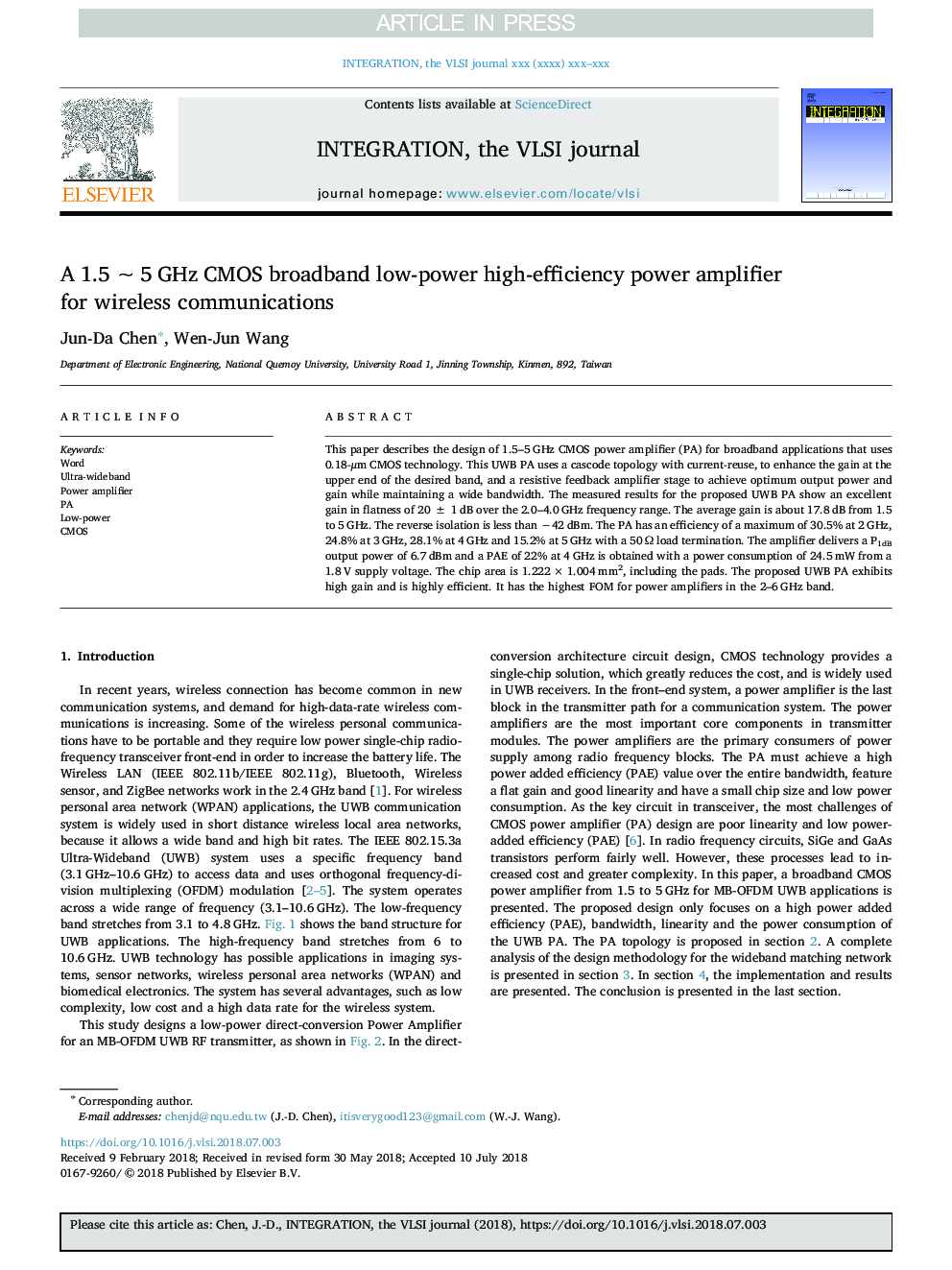
This paper describes the design of 1.5-5â¯GHz CMOS power amplifier (PA) for broadband applications that uses 0.18-μm CMOS technology. This UWB PA uses a cascode topology with current-reuse, to enhance the gain at the upper end of the desired band, and a resistive feedback amplifier stage to achieve optimum output power and gain while maintaining a wide bandwidth. The measured results for the proposed UWB PA show an excellent gain in flatness of 20â¯Â±â¯1â¯dB over the 2.0-4.0â¯GHz frequency range. The average gain is about 17.8â¯dB from 1.5 to 5â¯GHz. The reverse isolation is less than â42â¯dBm. The PA has an efficiency of a maximum of 30.5% at 2â¯GHz, 24.8% at 3â¯GHz, 28.1% at 4â¯GHz and 15.2% at 5â¯GHz with a 50â¯Î© load termination. The amplifier delivers a P1dB output power of 6.7â¯dBm and a PAE of 22% at 4â¯GHz is obtained with a power consumption of 24.5â¯mW from a 1.8â¯V supply voltage. The chip area is 1.222â¯Ãâ¯1.004â¯mm2, including the pads. The proposed UWB PA exhibits high gain and is highly efficient. It has the highest FOM for power amplifiers in the 2-6â¯GHz band.
Related Topics
Physical Sciences and Engineering
Computer Science
Hardware and Architecture
Authors
Jun-Da Chen, Wen-Jun Wang,
