| کد مقاله | کد نشریه | سال انتشار | مقاله انگلیسی | نسخه تمام متن |
|---|---|---|---|---|
| 1532615 | 996187 | 2011 | 40 صفحه PDF | دانلود رایگان |
عنوان انگلیسی مقاله ISI
Development of hafnium based high-k materials-A review
دانلود مقاله + سفارش ترجمه
دانلود مقاله ISI انگلیسی
رایگان برای ایرانیان
موضوعات مرتبط
مهندسی و علوم پایه
مهندسی مواد
مواد الکترونیکی، نوری و مغناطیسی
پیش نمایش صفحه اول مقاله

چکیده انگلیسی
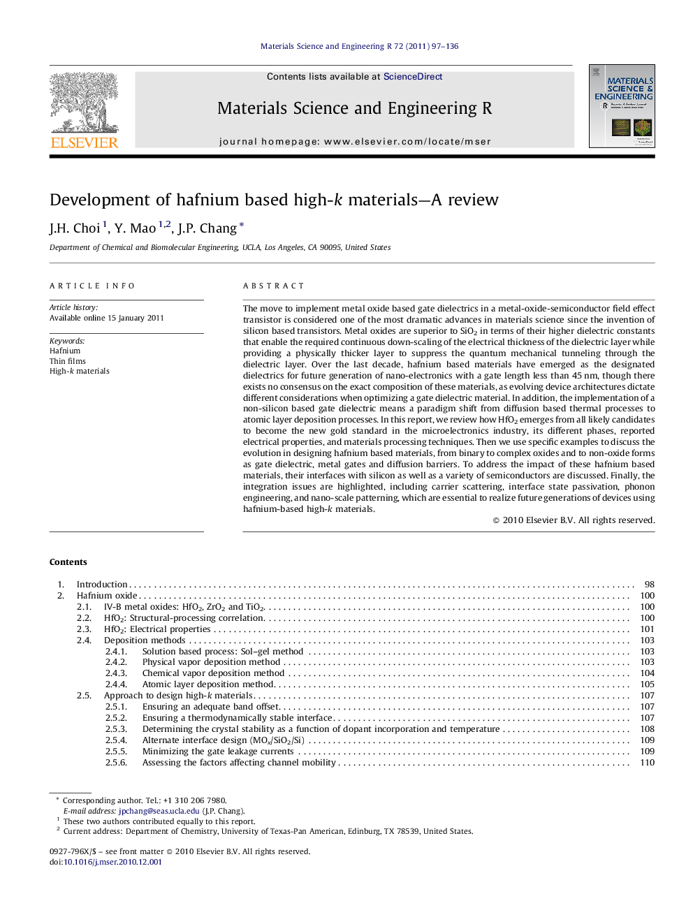
The move to implement metal oxide based gate dielectrics in a metal-oxide-semiconductor field effect transistor is considered one of the most dramatic advances in materials science since the invention of silicon based transistors. Metal oxides are superior to SiO2 in terms of their higher dielectric constants that enable the required continuous down-scaling of the electrical thickness of the dielectric layer while providing a physically thicker layer to suppress the quantum mechanical tunneling through the dielectric layer. Over the last decade, hafnium based materials have emerged as the designated dielectrics for future generation of nano-electronics with a gate length less than 45Â nm, though there exists no consensus on the exact composition of these materials, as evolving device architectures dictate different considerations when optimizing a gate dielectric material. In addition, the implementation of a non-silicon based gate dielectric means a paradigm shift from diffusion based thermal processes to atomic layer deposition processes. In this report, we review how HfO2 emerges from all likely candidates to become the new gold standard in the microelectronics industry, its different phases, reported electrical properties, and materials processing techniques. Then we use specific examples to discuss the evolution in designing hafnium based materials, from binary to complex oxides and to non-oxide forms as gate dielectric, metal gates and diffusion barriers. To address the impact of these hafnium based materials, their interfaces with silicon as well as a variety of semiconductors are discussed. Finally, the integration issues are highlighted, including carrier scattering, interface state passivation, phonon engineering, and nano-scale patterning, which are essential to realize future generations of devices using hafnium-based high-k materials.
ناشر
Database: Elsevier - ScienceDirect (ساینس دایرکت)
Journal: Materials Science and Engineering: R: Reports - Volume 72, Issue 6, 22 July 2011, Pages 97-136
Journal: Materials Science and Engineering: R: Reports - Volume 72, Issue 6, 22 July 2011, Pages 97-136
نویسندگان
J.H. Choi, Y. Mao, J.P. Chang,