| کد مقاله | کد نشریه | سال انتشار | مقاله انگلیسی | نسخه تمام متن |
|---|---|---|---|---|
| 239647 | 466199 | 2009 | 4 صفحه PDF | دانلود رایگان |

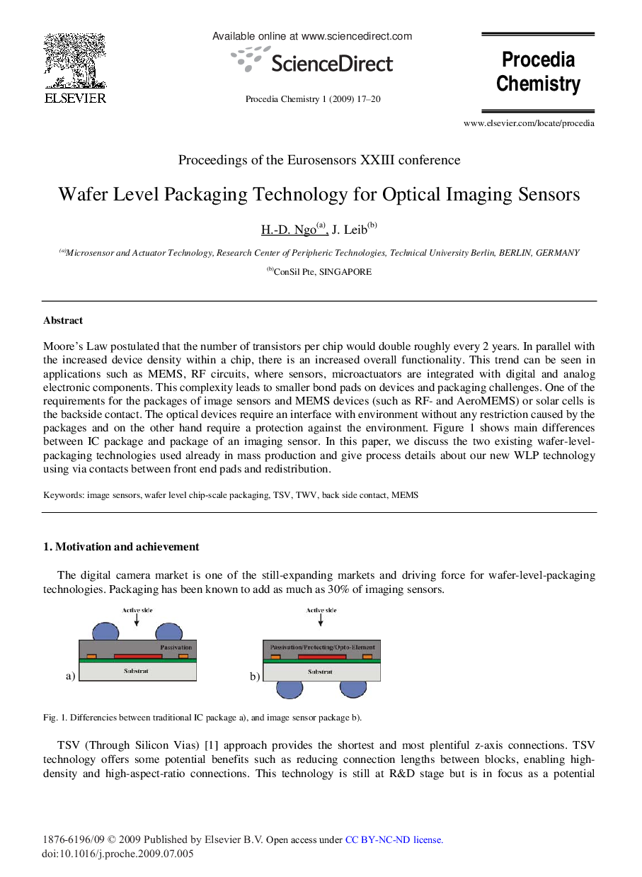
Moore’s Law postulated that the number of transistors per chip would double roughly every 2 years. In parallel with the increased device density within a chip, there is an increased overall functionality. This trend can be seen in applications such as MEMS, RF circuits, where sensors, microactuators are integrated with digital and analog electronic components. This complexity leads to smaller bond pads on devices and packaging challenges. One of the requirements for the packages of image sensors and MEMS devices (such as RF- and AeroMEMS) or solar cells is the backside contact. The optical devices require an interface with environment without any restriction caused by the packages and on the other hand require a protection against the environment. Figure 1 shows main differences between IC package and package of an imaging sensor. In this paper, we discuss the two existing wafer-level-packaging technologies used already in mass production and give process details about our new WLP technology using via contacts between front end pads and redistribution.
Journal: Procedia Chemistry - Volume 1, Issue 1, September 2009, Pages 17-20