| کد مقاله | کد نشریه | سال انتشار | مقاله انگلیسی | نسخه تمام متن |
|---|---|---|---|---|
| 9783891 | 1512026 | 2005 | 8 صفحه PDF | دانلود رایگان |
عنوان انگلیسی مقاله ISI
Advanced activation of ultra-shallow junctions using flash-assisted RTP
دانلود مقاله + سفارش ترجمه
دانلود مقاله ISI انگلیسی
رایگان برای ایرانیان
موضوعات مرتبط
مهندسی و علوم پایه
مهندسی مواد
مواد الکترونیکی، نوری و مغناطیسی
پیش نمایش صفحه اول مقاله

چکیده انگلیسی
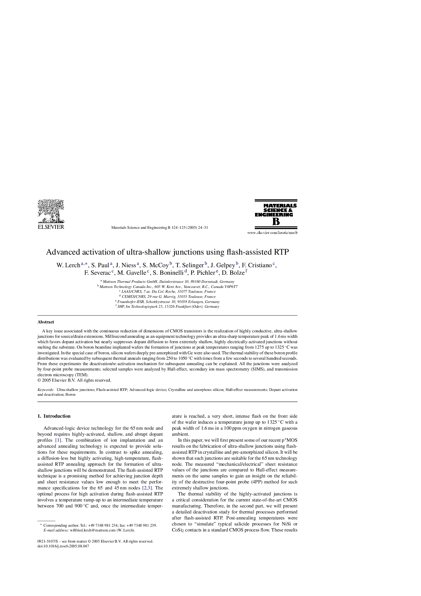
A key issue associated with the continuous reduction of dimensions of CMOS transistors is the realization of highly conductive, ultra-shallow junctions for source/drain extensions. Millisecond annealing as an equipment technology provides an ultra-sharp temperature peak of 1.6 ms width which favors dopant activation but nearly suppresses dopant diffusion to form extremely shallow, highly electrically-activated junctions without melting the substrate. On boron beamline implanted wafers the formation of junctions at peak temperatures ranging from 1275 up to 1325 °C was investigated. In the special case of boron, silicon wafers deeply pre-amorphized with Ge were also used. The thermal stability of these boron profile distributions was evaluated by subsequent thermal anneals ranging from 250 to 1050 °C with times from a few seconds to several hundred seconds. From these experiments the deactivation/re-activation mechanism for subsequent annealing can be explained. All the junctions were analyzed by four-point probe measurements; selected samples were analyzed by Hall-effect, secondary ion mass spectrometry (SIMS), and transmission electron microscopy (TEM).
ناشر
Database: Elsevier - ScienceDirect (ساینس دایرکت)
Journal: Materials Science and Engineering: B - Volumes 124â125, 5 December 2005, Pages 24-31
Journal: Materials Science and Engineering: B - Volumes 124â125, 5 December 2005, Pages 24-31
نویسندگان
W. Lerch, S. Paul, J. Niess, S. McCoy, T. Selinger, J. Gelpey, F. Cristiano, F. Severac, M. Gavelle, S. Boninelli, P. Pichler, D. Bolze,