| کد مقاله | کد نشریه | سال انتشار | مقاله انگلیسی | نسخه تمام متن |
|---|---|---|---|---|
| 10624402 | 989589 | 2016 | 7 صفحه PDF | دانلود رایگان |
عنوان انگلیسی مقاله ISI
Effect of bias voltage on microstructure and phase evolution of Cr-Mo-N coatings by an arc bonded sputter system
دانلود مقاله + سفارش ترجمه
دانلود مقاله ISI انگلیسی
رایگان برای ایرانیان
موضوعات مرتبط
مهندسی و علوم پایه
مهندسی مواد
سرامیک و کامپوزیت
پیش نمایش صفحه اول مقاله

چکیده انگلیسی
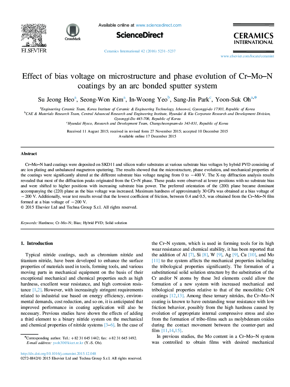
Cr-Mo-N hard coatings were deposited on SKD11 and silicon wafer substrates at various substrate bias voltages by hybrid PVD consisting of arc ion plating and unbalanced magnetron sputtering. The results showed that the microstructure, phase evolution, and mechanical properties of the coatings were significantly altered at the different substrate bias voltage ranging from 0 to â400Â V. The X-ray diffraction analysis results revealed that most of the diffraction peaks originated from the Cr-N phase. These peaks were observed at lower positions with no substrate bias and were shifted to higher positions with increasing substrate bias power. The preferred orientation of the (200) plane became dominant accompanying the (220) plane as the bias voltage was increased. Maximum hardness of approximately 30Â GPa was obtained at a bias voltage of â200Â V. Additionally, wear test results reveal that the lowest coefficient of friction, between 0.4 and 0.5, was obtained from the Cr-Mo-N film formed at a bias voltage of â200Â V.
ناشر
Database: Elsevier - ScienceDirect (ساینس دایرکت)
Journal: Ceramics International - Volume 42, Issue 4, March 2016, Pages 5231-5237
Journal: Ceramics International - Volume 42, Issue 4, March 2016, Pages 5231-5237
نویسندگان
Su Jeong Heo, Seong-Won Kim, In-Woong Yeo, Sang-Jin Park, Yoon-Suk Oh,