| کد مقاله | کد نشریه | سال انتشار | مقاله انگلیسی | نسخه تمام متن |
|---|---|---|---|---|
| 11016488 | 1777112 | 2018 | 13 صفحه PDF | دانلود رایگان |
عنوان انگلیسی مقاله ISI
Failure analysis on 14â¯nm FinFET devices with ESD CDM failure
دانلود مقاله + سفارش ترجمه
دانلود مقاله ISI انگلیسی
رایگان برای ایرانیان
کلمات کلیدی
موضوعات مرتبط
مهندسی و علوم پایه
مهندسی کامپیوتر
سخت افزارها و معماری
پیش نمایش صفحه اول مقاله

چکیده انگلیسی
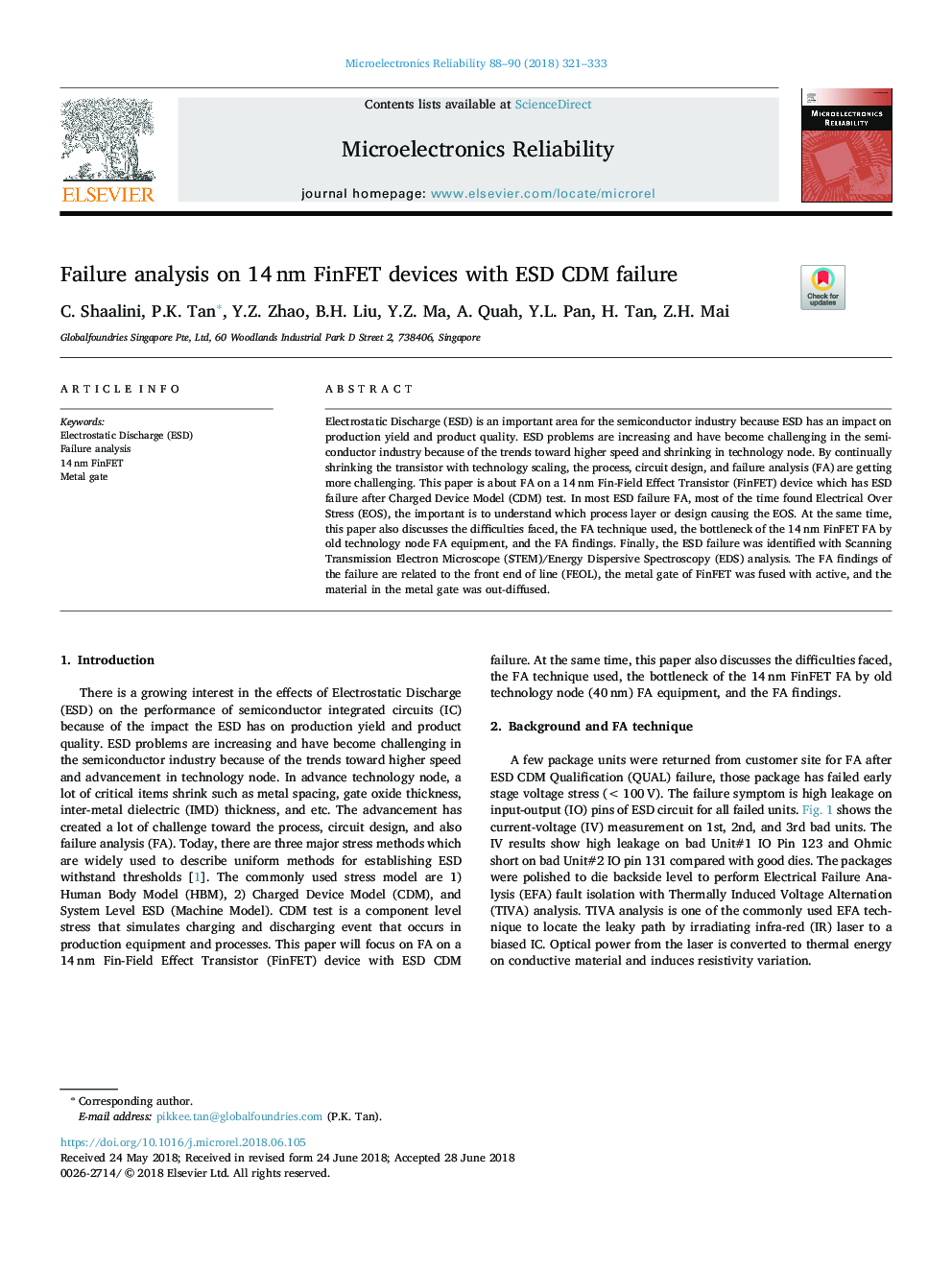
Electrostatic Discharge (ESD) is an important area for the semiconductor industry because ESD has an impact on production yield and product quality. ESD problems are increasing and have become challenging in the semiconductor industry because of the trends toward higher speed and shrinking in technology node. By continually shrinking the transistor with technology scaling, the process, circuit design, and failure analysis (FA) are getting more challenging. This paper is about FA on a 14â¯nm Fin-Field Effect Transistor (FinFET) device which has ESD failure after Charged Device Model (CDM) test. In most ESD failure FA, most of the time found Electrical Over Stress (EOS), the important is to understand which process layer or design causing the EOS. At the same time, this paper also discusses the difficulties faced, the FA technique used, the bottleneck of the 14â¯nm FinFET FA by old technology node FA equipment, and the FA findings. Finally, the ESD failure was identified with Scanning Transmission Electron Microscope (STEM)/Energy Dispersive Spectroscopy (EDS) analysis. The FA findings of the failure are related to the front end of line (FEOL), the metal gate of FinFET was fused with active, and the material in the metal gate was out-diffused.
ناشر
Database: Elsevier - ScienceDirect (ساینس دایرکت)
Journal: Microelectronics Reliability - Volumes 88â90, September 2018, Pages 321-333
Journal: Microelectronics Reliability - Volumes 88â90, September 2018, Pages 321-333
نویسندگان
C. Shaalini, P.K. Tan, Y.Z. Zhao, B.H. Liu, Y.Z. Ma, A. Quah, Y.L. Pan, H. Tan, Z.H. Mai,