| کد مقاله | کد نشریه | سال انتشار | مقاله انگلیسی | نسخه تمام متن |
|---|---|---|---|---|
| 6946709 | 1450545 | 2015 | 8 صفحه PDF | دانلود رایگان |
عنوان انگلیسی مقاله ISI
Reliability studies of vertical GaN devices based on bulk GaN substrates
دانلود مقاله + سفارش ترجمه
دانلود مقاله ISI انگلیسی
رایگان برای ایرانیان
کلمات کلیدی
موضوعات مرتبط
مهندسی و علوم پایه
مهندسی کامپیوتر
سخت افزارها و معماری
پیش نمایش صفحه اول مقاله

چکیده انگلیسی
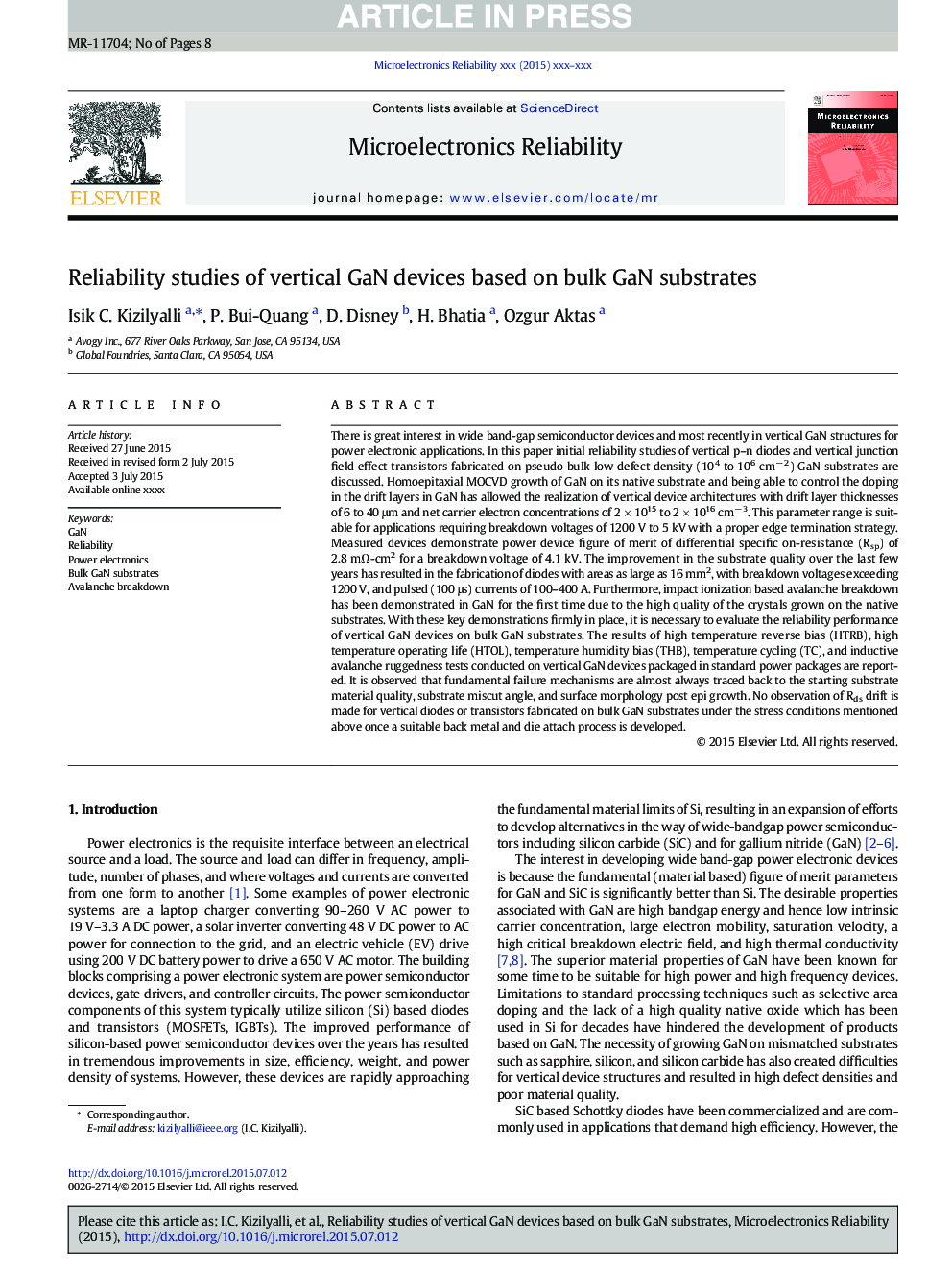
There is great interest in wide band-gap semiconductor devices and most recently in vertical GaN structures for power electronic applications. In this paper initial reliability studies of vertical p-n diodes and vertical junction field effect transistors fabricated on pseudo bulk low defect density (104 to 106 cmâ 2) GaN substrates are discussed. Homoepitaxial MOCVD growth of GaN on its native substrate and being able to control the doping in the drift layers in GaN has allowed the realization of vertical device architectures with drift layer thicknesses of 6 to 40 μm and net carrier electron concentrations of 2 Ã 1015 to 2 Ã 1016 cmâ 3. This parameter range is suitable for applications requiring breakdown voltages of 1200 V to 5 kV with a proper edge termination strategy. Measured devices demonstrate power device figure of merit of differential specific on-resistance (Rsp) of 2.8 mΩ-cm2 for a breakdown voltage of 4.1 kV. The improvement in the substrate quality over the last few years has resulted in the fabrication of diodes with areas as large as 16 mm2, with breakdown voltages exceeding 1200 V, and pulsed (100 μs) currents of 100-400 A. Furthermore, impact ionization based avalanche breakdown has been demonstrated in GaN for the first time due to the high quality of the crystals grown on the native substrates. With these key demonstrations firmly in place, it is necessary to evaluate the reliability performance of vertical GaN devices on bulk GaN substrates. The results of high temperature reverse bias (HTRB), high temperature operating life (HTOL), temperature humidity bias (THB), temperature cycling (TC), and inductive avalanche ruggedness tests conducted on vertical GaN devices packaged in standard power packages are reported. It is observed that fundamental failure mechanisms are almost always traced back to the starting substrate material quality, substrate miscut angle, and surface morphology post epi growth. No observation of Rds drift is made for vertical diodes or transistors fabricated on bulk GaN substrates under the stress conditions mentioned above once a suitable back metal and die attach process is developed.
ناشر
Database: Elsevier - ScienceDirect (ساینس دایرکت)
Journal: Microelectronics Reliability - Volume 55, Issues 9â10, AugustâSeptember 2015, Pages 1654-1661
Journal: Microelectronics Reliability - Volume 55, Issues 9â10, AugustâSeptember 2015, Pages 1654-1661
نویسندگان
Isik C. Kizilyalli, P. Bui-Quang, D. Disney, H. Bhatia, Ozgur Aktas,