| کد مقاله | کد نشریه | سال انتشار | مقاله انگلیسی | نسخه تمام متن |
|---|---|---|---|---|
| 542727 | 871569 | 2006 | 6 صفحه PDF | دانلود رایگان |
عنوان انگلیسی مقاله ISI
Formation of a buried collector layer in RF-bipolar devices by ion implantation
دانلود مقاله + سفارش ترجمه
دانلود مقاله ISI انگلیسی
رایگان برای ایرانیان
موضوعات مرتبط
مهندسی و علوم پایه
مهندسی کامپیوتر
سخت افزارها و معماری
پیش نمایش صفحه اول مقاله

چکیده انگلیسی
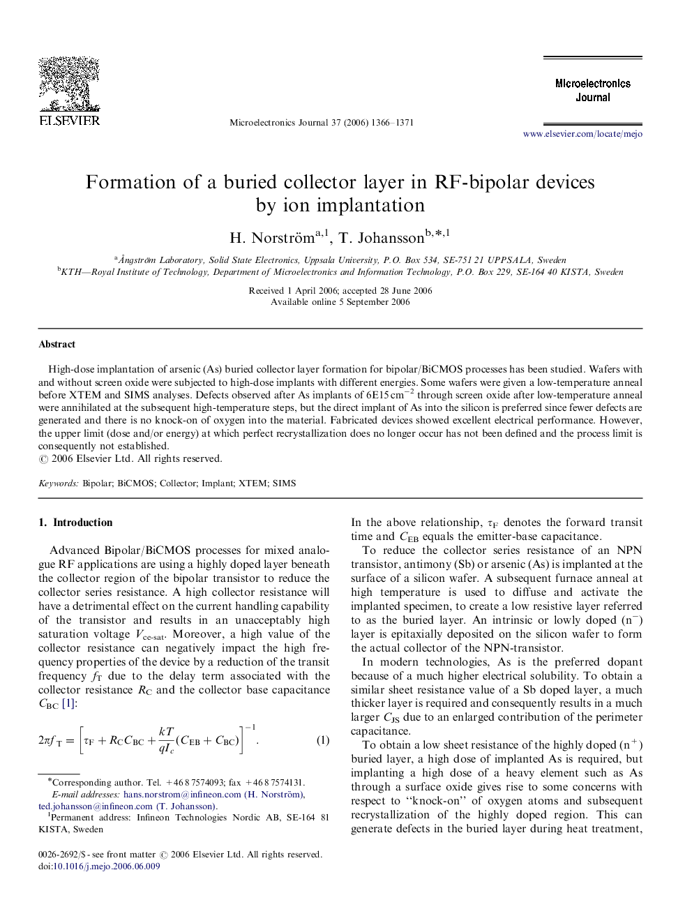
High-dose implantation of arsenic (As) buried collector layer formation for bipolar/BiCMOS processes has been studied. Wafers with and without screen oxide were subjected to high-dose implants with different energies. Some wafers were given a low-temperature anneal before XTEM and SIMS analyses. Defects observed after As implants of 6E15Â cmâ2 through screen oxide after low-temperature anneal were annihilated at the subsequent high-temperature steps, but the direct implant of As into the silicon is preferred since fewer defects are generated and there is no knock-on of oxygen into the material. Fabricated devices showed excellent electrical performance. However, the upper limit (dose and/or energy) at which perfect recrystallization does no longer occur has not been defined and the process limit is consequently not established.
ناشر
Database: Elsevier - ScienceDirect (ساینس دایرکت)
Journal: Microelectronics Journal - Volume 37, Issue 11, November 2006, Pages 1366-1371
Journal: Microelectronics Journal - Volume 37, Issue 11, November 2006, Pages 1366-1371
نویسندگان
H. Norström, T. Johansson,