| کد مقاله | کد نشریه | سال انتشار | مقاله انگلیسی | نسخه تمام متن |
|---|---|---|---|---|
| 9594613 | 1507971 | 2005 | 12 صفحه PDF | دانلود رایگان |
عنوان انگلیسی مقاله ISI
Initial growth processes of ultra-thin Ni-layers on Si(1Â 1Â 1) and electronic structure of epitaxially grown NiSi2
دانلود مقاله + سفارش ترجمه
دانلود مقاله ISI انگلیسی
رایگان برای ایرانیان
کلمات کلیدی
موضوعات مرتبط
مهندسی و علوم پایه
شیمی
شیمی تئوریک و عملی
پیش نمایش صفحه اول مقاله

چکیده انگلیسی
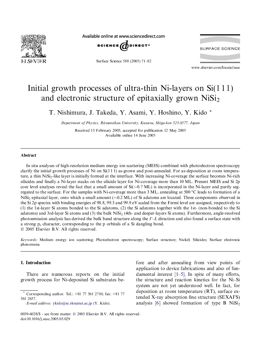
In situ analyses of high-resolution medium energy ion scattering (MEIS) combined with photoelectron spectroscopy clarify the initial growth processes of Ni on Si(1 1 1) as-grown and post-annealed. For as-deposition at room temperature, a thin NiSi2-like layer is initially formed at the interface. With increasing Ni-coverage the surface becomes Ni-rich silicides and finally a Ni-layer stacks on the silicide layer for Ni-coverage more than 10 ML. Present MEIS and Si 2p core level analyses reveal the fact that a small amount of Si(â¼0.7 ML) is incorporated in the Ni-layer and partly segregated to the surface. For the samples with Ni-coverage more than 3 ML, annealing at 500 °C leads to formation of a NiSi2 epitaxial layer, onto which a small amount (â¼0.2 ML) of Si adatoms are located. Three components observed in the Si 2p spectra with binding energies of 98.8, 99.3 and 99.9 eV scaled from the Fermi level are assigned, respectively to (1) the 1st-layer Si atoms bonded to the Si adatoms, (2) the Si adatoms together with the 1st- (non-bonded to the Si adatoms) and 3rd-layer Si atoms and (3) the bulk NiSi2 (4th- and deeper-layers Si atoms). Furthermore, angle-resolved photoemission analysis has derived the bulk band structure along the Î-L direction and also found a surface state with a strong pz character, corresponding to the p orbitals of a Si dangling bond.
ناشر
Database: Elsevier - ScienceDirect (ساینس دایرکت)
Journal: Surface Science - Volume 588, Issues 1â3, 20 August 2005, Pages 71-82
Journal: Surface Science - Volume 588, Issues 1â3, 20 August 2005, Pages 71-82
نویسندگان
T. Nishimura, J. Takeda, Y. Asami, Y. Hoshino, Y. Kido,