| کد مقاله | کد نشریه | سال انتشار | مقاله انگلیسی | نسخه تمام متن |
|---|---|---|---|---|
| 9817739 | 1518771 | 2005 | 7 صفحه PDF | دانلود رایگان |
عنوان انگلیسی مقاله ISI
Nickel silicide formation on shallow junctions
دانلود مقاله + سفارش ترجمه
دانلود مقاله ISI انگلیسی
رایگان برای ایرانیان
کلمات کلیدی
موضوعات مرتبط
مهندسی و علوم پایه
مهندسی مواد
سطوح، پوششها و فیلمها
پیش نمایش صفحه اول مقاله

چکیده انگلیسی
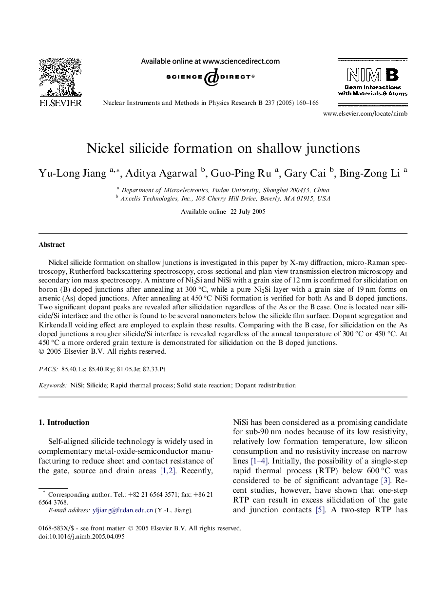
Nickel silicide formation on shallow junctions is investigated in this paper by X-ray diffraction, micro-Raman spectroscopy, Rutherford backscattering spectroscopy, cross-sectional and plan-view transmission electron microscopy and secondary ion mass spectroscopy. A mixture of Ni2Si and NiSi with a grain size of 12 nm is confirmed for silicidation on boron (B) doped junctions after annealing at 300 °C, while a pure Ni2Si layer with a grain size of 19 nm forms on arsenic (As) doped junctions. After annealing at 450 °C NiSi formation is verified for both As and B doped junctions. Two significant dopant peaks are revealed after silicidation regardless of the As or the B case. One is located near silicide/Si interface and the other is found to be several nanometers below the silicide film surface. Dopant segregation and Kirkendall voiding effect are employed to explain these results. Comparing with the B case, for silicidation on the As doped junctions a rougher silicide/Si interface is revealed regardless of the anneal temperature of 300 °C or 450 °C. At 450 °C a more ordered grain texture is demonstrated for silicidation on the B doped junctions.
ناشر
Database: Elsevier - ScienceDirect (ساینس دایرکت)
Journal: Nuclear Instruments and Methods in Physics Research Section B: Beam Interactions with Materials and Atoms - Volume 237, Issues 1â2, August 2005, Pages 160-166
Journal: Nuclear Instruments and Methods in Physics Research Section B: Beam Interactions with Materials and Atoms - Volume 237, Issues 1â2, August 2005, Pages 160-166
نویسندگان
Yu-Long Jiang, Aditya Agarwal, Guo-Ping Ru, Gary Cai, Bing-Zong Li,