| کد مقاله | کد نشریه | سال انتشار | مقاله انگلیسی | نسخه تمام متن |
|---|---|---|---|---|
| 11003597 | 1461359 | 2018 | 10 صفحه PDF | دانلود رایگان |
عنوان انگلیسی مقاله ISI
Characterization of N-type and P-type Aluminum Antimonides on Si substrates for room-temperature optoelectronic devices
دانلود مقاله + سفارش ترجمه
دانلود مقاله ISI انگلیسی
رایگان برای ایرانیان
کلمات کلیدی
موضوعات مرتبط
مهندسی و علوم پایه
سایر رشته های مهندسی
مهندسی برق و الکترونیک
پیش نمایش صفحه اول مقاله

چکیده انگلیسی
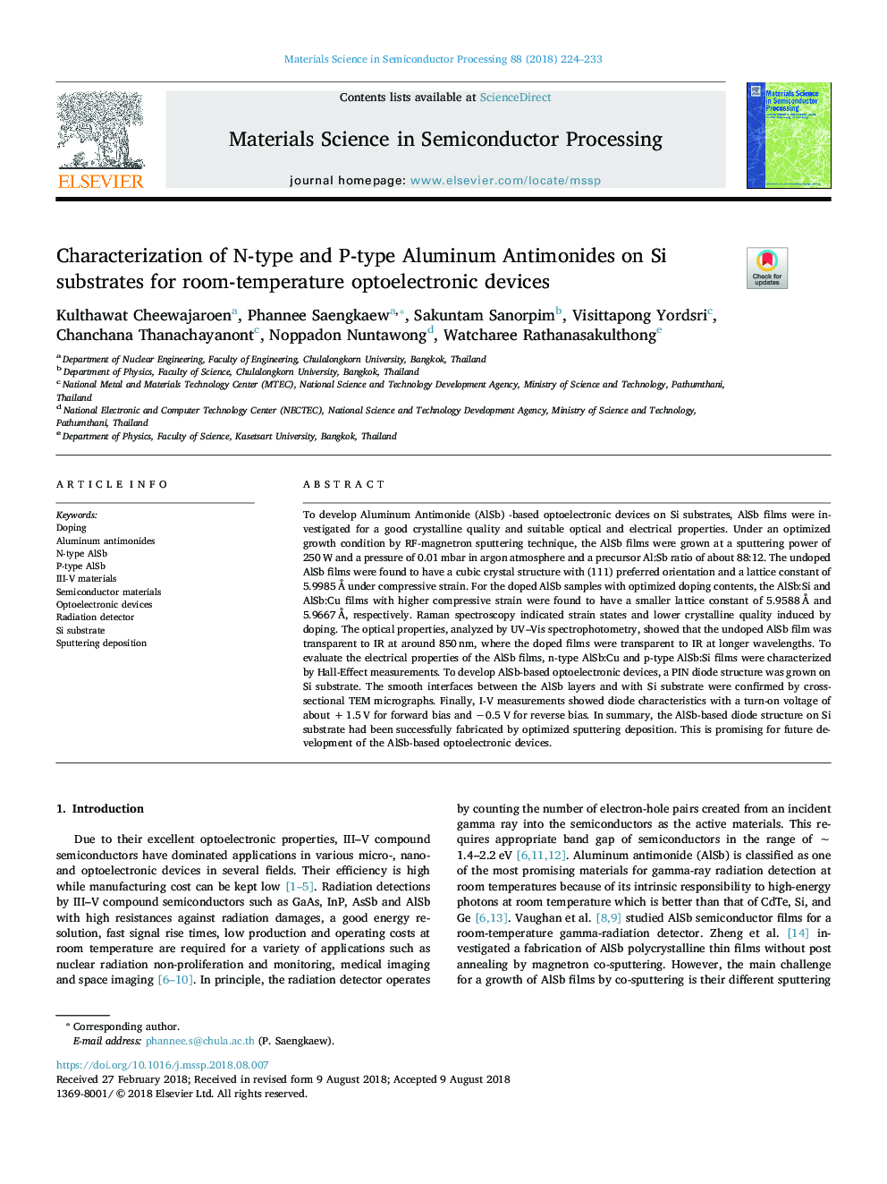
To develop Aluminum Antimonide (AlSb) -based optoelectronic devices on Si substrates, AlSb films were investigated for a good crystalline quality and suitable optical and electrical properties. Under an optimized growth condition by RF-magnetron sputtering technique, the AlSb films were grown at a sputtering power of 250â¯W and a pressure of 0.01 mbar in argon atmosphere and a precursor Al:Sb ratio of about 88:12. The undoped AlSb films were found to have a cubic crystal structure with (111) preferred orientation and a lattice constant of 5.9985â¯Ã
under compressive strain. For the doped AlSb samples with optimized doping contents, the AlSb:Si and AlSb:Cu films with higher compressive strain were found to have a smaller lattice constant of 5.9588â¯Ã
and 5.9667â¯Ã
, respectively. Raman spectroscopy indicated strain states and lower crystalline quality induced by doping. The optical properties, analyzed by UV-Vis spectrophotometry, showed that the undoped AlSb film was transparent to IR at around 850â¯nm, where the doped films were transparent to IR at longer wavelengths. To evaluate the electrical properties of the AlSb films, n-type AlSb:Cu and p-type AlSb:Si films were characterized by Hall-Effect measurements. To develop AlSb-based optoelectronic devices, a PIN diode structure was grown on Si substrate. The smooth interfaces between the AlSb layers and with Si substrate were confirmed by cross-sectional TEM micrographs. Finally, I-V measurements showed diode characteristics with a turn-on voltage of about +â¯1.5â¯V for forward bias and â0.5â¯V for reverse bias. In summary, the AlSb-based diode structure on Si substrate had been successfully fabricated by optimized sputtering deposition. This is promising for future development of the AlSb-based optoelectronic devices.
ناشر
Database: Elsevier - ScienceDirect (ساینس دایرکت)
Journal: Materials Science in Semiconductor Processing - Volume 88, December 2018, Pages 224-233
Journal: Materials Science in Semiconductor Processing - Volume 88, December 2018, Pages 224-233
نویسندگان
Kulthawat Cheewajaroen, Phannee Saengkaew, Sakuntam Sanorpim, Visittapong Yordsri, Chanchana Thanachayanont, Noppadon Nuntawong, Watcharee Rathanasakulthong,