| کد مقاله | کد نشریه | سال انتشار | مقاله انگلیسی | نسخه تمام متن |
|---|---|---|---|---|
| 5006023 | 1461379 | 2017 | 5 صفحه PDF | دانلود رایگان |
عنوان انگلیسی مقاله ISI
Fabrication of multi-layer Bi2Se3 devices and observation of anomalous electrical transport behaviors
دانلود مقاله + سفارش ترجمه
دانلود مقاله ISI انگلیسی
رایگان برای ایرانیان
موضوعات مرتبط
مهندسی و علوم پایه
سایر رشته های مهندسی
مهندسی برق و الکترونیک
پیش نمایش صفحه اول مقاله

چکیده انگلیسی
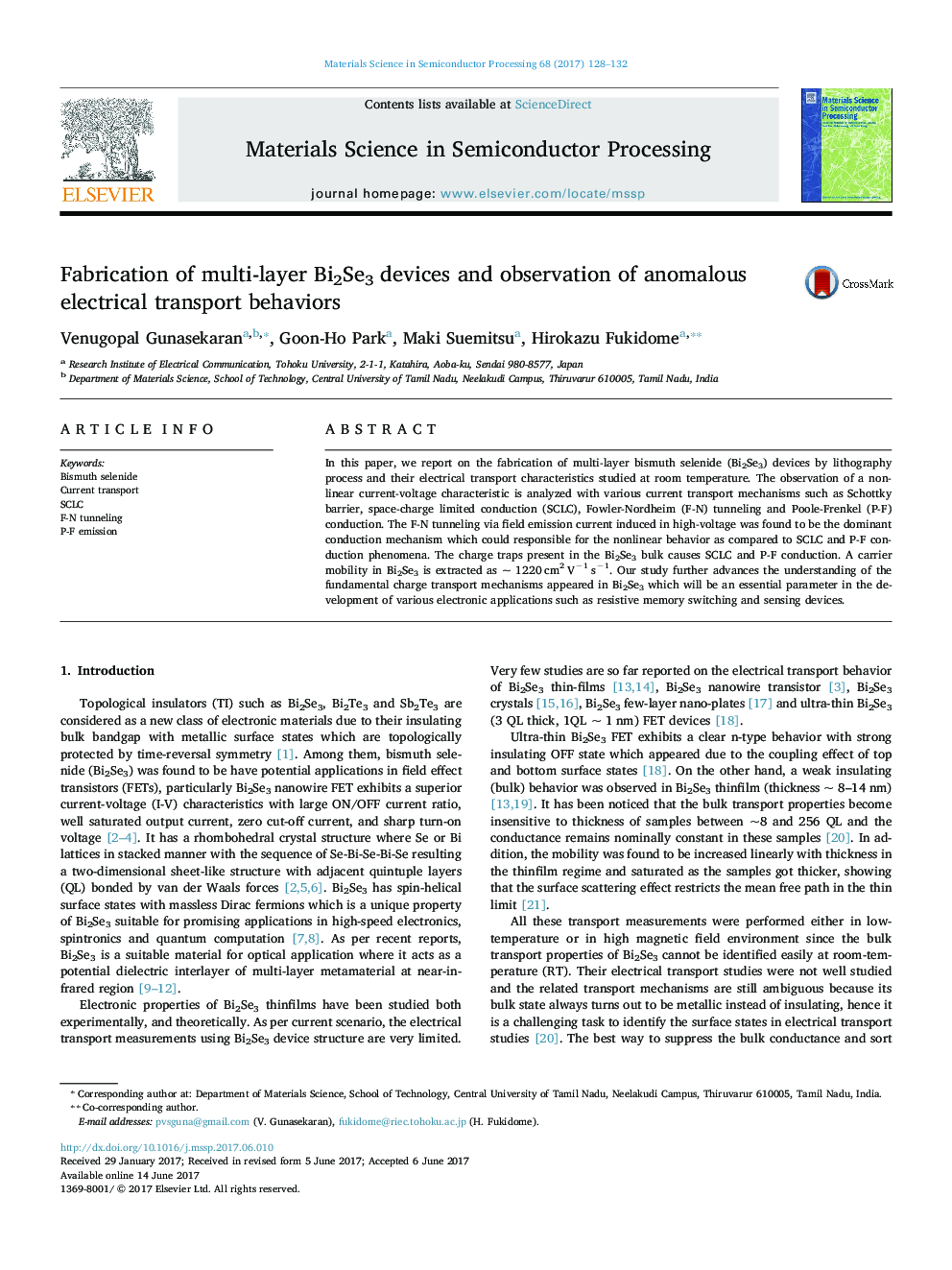
In this paper, we report on the fabrication of multi-layer bismuth selenide (Bi2Se3) devices by lithography process and their electrical transport characteristics studied at room temperature. The observation of a non-linear current-voltage characteristic is analyzed with various current transport mechanisms such as Schottky barrier, space-charge limited conduction (SCLC), Fowler-Nordheim (F-N) tunneling and Poole-Frenkel (P-F) conduction. The F-N tunneling via field emission current induced in high-voltage was found to be the dominant conduction mechanism which could responsible for the nonlinear behavior as compared to SCLC and P-F conduction phenomena. The charge traps present in the Bi2Se3 bulk causes SCLC and P-F conduction. A carrier mobility in Bi2Se3 is extracted as ~ 1220Â cm2Â Vâ1Â sâ1. Our study further advances the understanding of the fundamental charge transport mechanisms appeared in Bi2Se3 which will be an essential parameter in the development of various electronic applications such as resistive memory switching and sensing devices.
ناشر
Database: Elsevier - ScienceDirect (ساینس دایرکت)
Journal: Materials Science in Semiconductor Processing - Volume 68, September 2017, Pages 128-132
Journal: Materials Science in Semiconductor Processing - Volume 68, September 2017, Pages 128-132
نویسندگان
Venugopal Gunasekaran, Goon-Ho Park, Maki Suemitsu, Hirokazu Fukidome,