| کد مقاله | کد نشریه | سال انتشار | مقاله انگلیسی | نسخه تمام متن |
|---|---|---|---|---|
| 545286 | 871814 | 2006 | 7 صفحه PDF | دانلود رایگان |
عنوان انگلیسی مقاله ISI
The etchback approach: Enlarged process window for MuGFET gate etching
دانلود مقاله + سفارش ترجمه
دانلود مقاله ISI انگلیسی
رایگان برای ایرانیان
کلمات کلیدی
موضوعات مرتبط
مهندسی و علوم پایه
مهندسی کامپیوتر
سخت افزارها و معماری
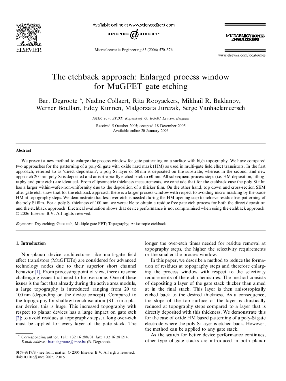
پیش نمایش صفحه اول مقاله

چکیده انگلیسی
We present a new method to enlarge the process window for gate patterning on a surface with high topography. We have compared two approaches for the patterning of a poly-Si gate with oxide hard mask (HM) as used in multi-gate field effect transistors. In the first approach, referred to as 'direct deposition', a poly-Si layer of 60Â nm is deposited on the substrate, whereas in the second, and new approach 200Â nm poly-Si is deposited and anisotropically etched back to 60Â nm. All subsequent process steps (i.e. HM deposition, lithography and gate etch) are identical. From ellipsometric thickness measurements, we conclude that for the etchback case the poly-Si film has a larger within-wafer-non-uniformity due to the deposition of a thicker film. On the other hand, top down and cross-section SEM after gate etch show that for the etchback approach there is a larger process window with respect to avoiding micro-masking by the oxide HM at topography steps. We demonstrate that less over-etch is needed during the HM opening step to achieve residue free patterning of the poly-Si film. For a poly-Si thickness of 100Â nm, we were able to obtain a residue free gate etch process for both the direct deposition and the etchback approach. Electrical evaluation shows that device performance is not compromised when using the etchback approach.
ناشر
Database: Elsevier - ScienceDirect (ساینس دایرکت)
Journal: Microelectronic Engineering - Volume 83, Issue 3, March 2006, Pages 570-576
Journal: Microelectronic Engineering - Volume 83, Issue 3, March 2006, Pages 570-576
نویسندگان
Bart Degroote, Nadine Collaert, Rita Rooyackers, Mikhail R. Baklanov, Werner Boullart, Eddy Kunnen, Malgorzata Jurczak, Serge Vanhaelemeersch,