| کد مقاله | کد نشریه | سال انتشار | مقاله انگلیسی | نسخه تمام متن |
|---|---|---|---|---|
| 7117697 | 1461366 | 2018 | 5 صفحه PDF | دانلود رایگان |
عنوان انگلیسی مقاله ISI
Low resistance Ga-doped ZnO ohmic contact to p-GaN by reducing the sputtering power
دانلود مقاله + سفارش ترجمه
دانلود مقاله ISI انگلیسی
رایگان برای ایرانیان
کلمات کلیدی
موضوعات مرتبط
مهندسی و علوم پایه
سایر رشته های مهندسی
مهندسی برق و الکترونیک
پیش نمایش صفحه اول مقاله

چکیده انگلیسی
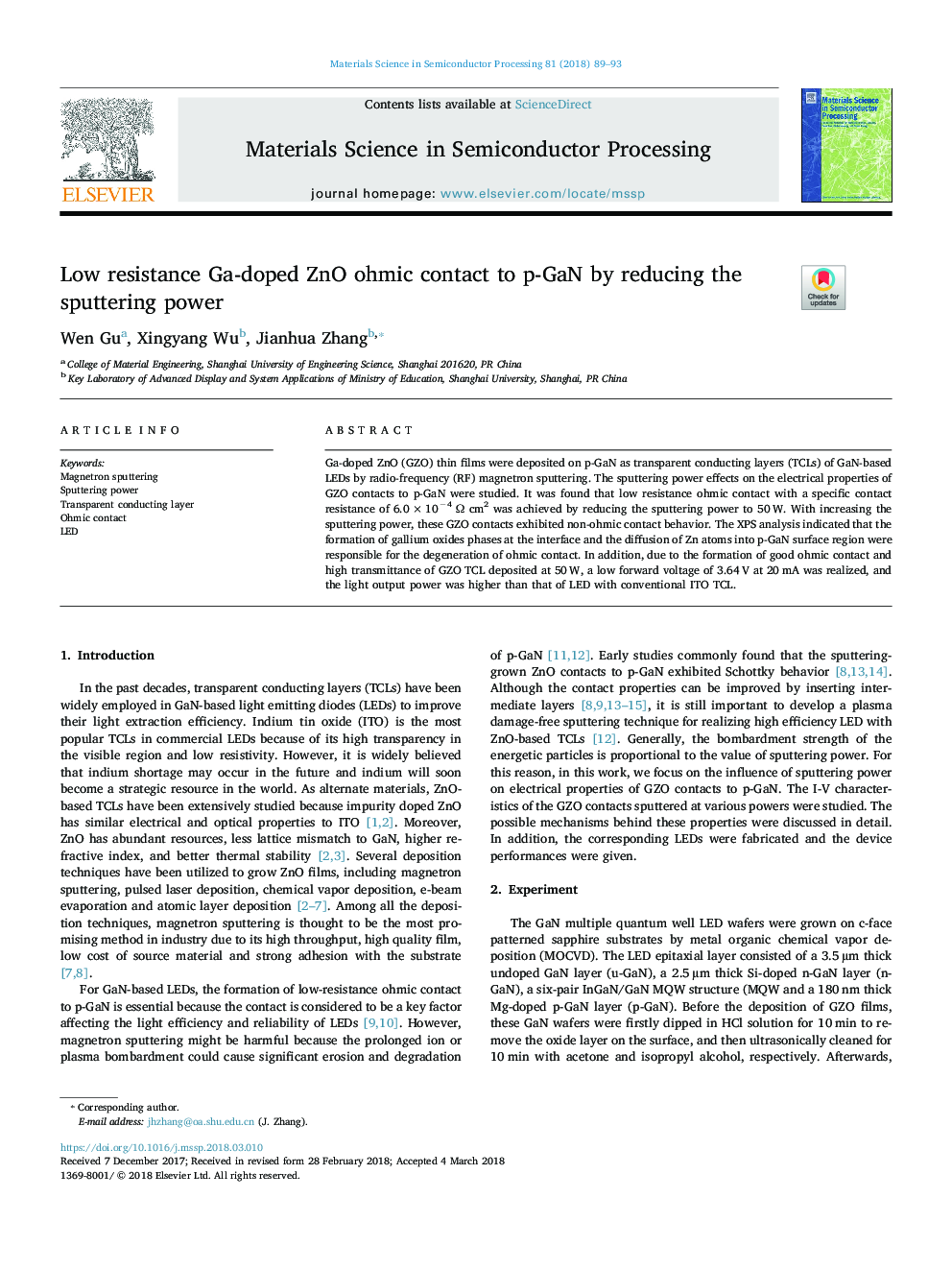
Ga-doped ZnO (GZO) thin films were deposited on p-GaN as transparent conducting layers (TCLs) of GaN-based LEDs by radio-frequency (RF) magnetron sputtering. The sputtering power effects on the electrical properties of GZO contacts to p-GaN were studied. It was found that low resistance ohmic contact with a specific contact resistance of 6.0â¯Ãâ¯10â4 Ω cm2 was achieved by reducing the sputtering power to 50â¯W. With increasing the sputtering power, these GZO contacts exhibited non-ohmic contact behavior. The XPS analysis indicated that the formation of gallium oxides phases at the interface and the diffusion of Zn atoms into p-GaN surface region were responsible for the degeneration of ohmic contact. In addition, due to the formation of good ohmic contact and high transmittance of GZO TCL deposited at 50â¯W, a low forward voltage of 3.64â¯V at 20â¯mA was realized, and the light output power was higher than that of LED with conventional ITO TCL.
ناشر
Database: Elsevier - ScienceDirect (ساینس دایرکت)
Journal: Materials Science in Semiconductor Processing - Volume 81, July 2018, Pages 89-93
Journal: Materials Science in Semiconductor Processing - Volume 81, July 2018, Pages 89-93
نویسندگان
Wen Gu, Xingyang Wu, Jianhua Zhang,