| کد مقاله | کد نشریه | سال انتشار | مقاله انگلیسی | نسخه تمام متن |
|---|---|---|---|---|
| 1552466 | 1513203 | 2016 | 9 صفحه PDF | دانلود رایگان |
عنوان انگلیسی مقاله ISI
Modeling and estimation of process-induced stress in the nanowire field-effect-transistors (NW-FETs) on Insulator-on-Silicon substrates with high-k gate-dielectrics
دانلود مقاله + سفارش ترجمه
دانلود مقاله ISI انگلیسی
رایگان برای ایرانیان
کلمات کلیدی
موضوعات مرتبط
مهندسی و علوم پایه
مهندسی مواد
مواد الکترونیکی، نوری و مغناطیسی
پیش نمایش صفحه اول مقاله

چکیده انگلیسی
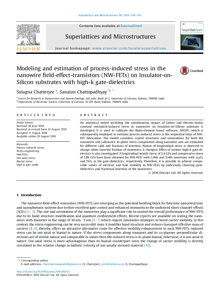
An analytical model including the simultaneous impact of lattice and thermo-elastic constant mismatch-induced stress in nanowires on Insulator-on-Silicon substrate is developed. It is used to calibrate the finite-element based software, ANSYS, which is subsequently employed to estimate process-induced stress in the sequential steps of NW-FET fabrication. The model considers crystal structures and orientations for both the nanowires and substrates. In-plane stress components along nanowire-axis are estimated for different radii and fractions of insertion. Nature of longitudinal stress is observed to change when inserted fraction of nanowires is changed. Effect of various high-k gate-dielectrics is also investigated. A longitudinal tensile stress of 2.4Â GPa and compressive stress of 1.89Â GPa have been obtained for NW-FETs with 1/4th and 3/4th insertions with La2O3 and TiO2 as the gate-dielectrics, respectively. Therefore, it is possible to achieve comparable values of electron and hole mobility in NW-FETs by judiciously choosing gate-dielectrics and fractional insertion of the nanowires.
ناشر
Database: Elsevier - ScienceDirect (ساینس دایرکت)
Journal: Superlattices and Microstructures - Volume 98, October 2016, Pages 194-202
Journal: Superlattices and Microstructures - Volume 98, October 2016, Pages 194-202
نویسندگان
Sulagna Chatterjee, Sanatan Chattopadhyay,