| کد مقاله | کد نشریه | سال انتشار | مقاله انگلیسی | نسخه تمام متن |
|---|---|---|---|---|
| 1543717 | 1512869 | 2016 | 4 صفحه PDF | دانلود رایگان |

• GaN nanowires containing structure defects were synthesized through a CVD process.
• GaN nanowires with stacking faults show strong yellow emission in visible range.
• The origin of yellow band emission in GaN nanowires is experimentally evidenced.
GaN nanowires with large yield are directly synthesized by simply ammoniating the gallium oxide powders in the presence of ammonia gas at 1000 °C, under the assistance of Au nanocatalysts. The microstructure and crystallinity of as-synthesized GaN nanowires are well studied by using high-resolution transmission electron microscope (HRTEM) and some structural defects such as stacking faults are found in the GaN nano-crystal. Cathodoluminescence measurement shows that a strong near-band-edge (NBE) emission band centered at 384 nm and a broad yellow band in the range of 500–800 nm are observed. Finally, the growth mechanism and possible optical emission process of GaN nanowires are discussed.
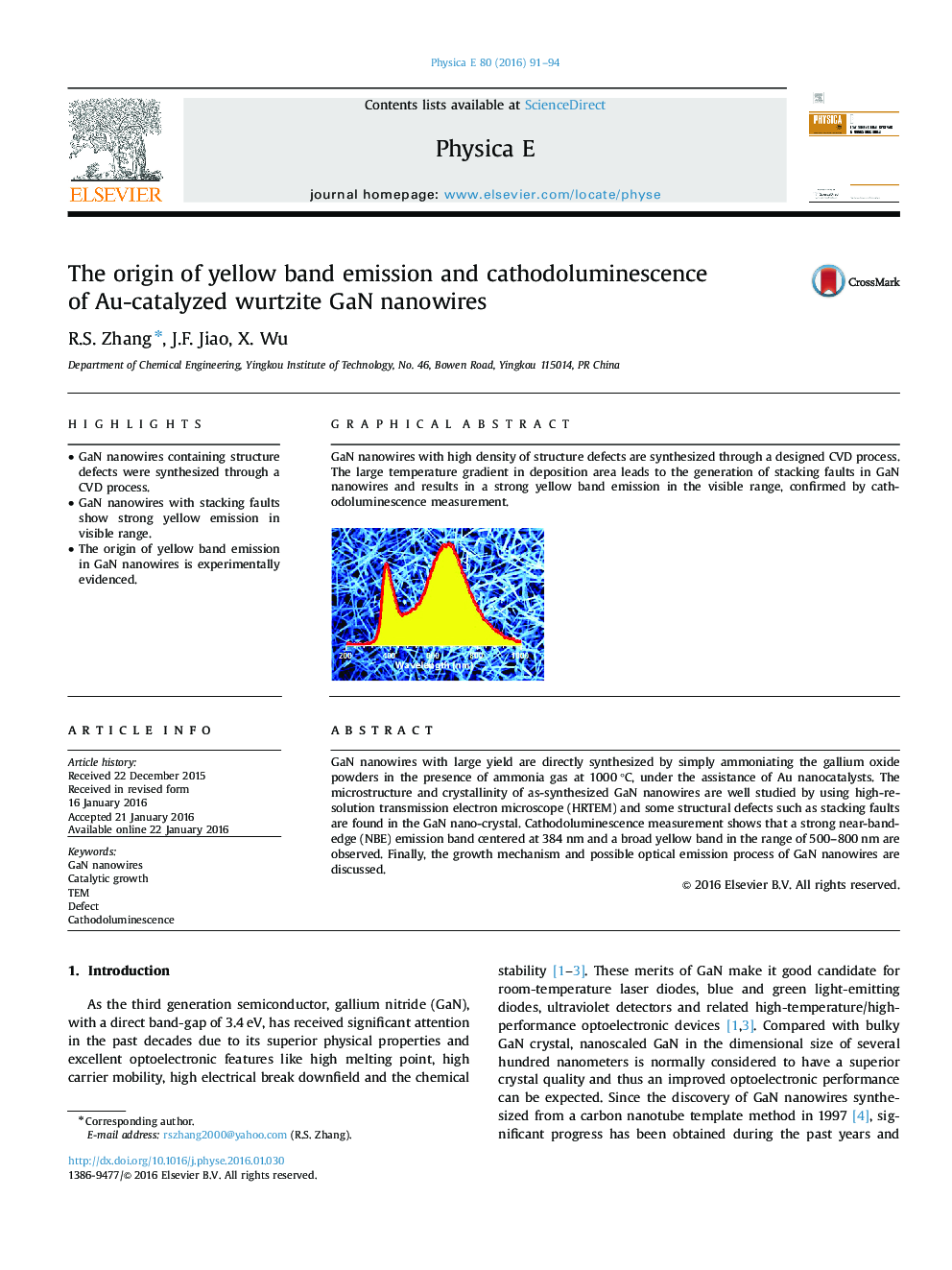
GaN nanowires with high density of structure defects are synthesized through a designed CVD process. The large temperature gradient in deposition area leads to the generation of stacking faults in GaN nanowires and results in a strong yellow band emission in the visible range, confirmed by cathodoluminescence measurement.Figure optionsDownload as PowerPoint slide
Journal: Physica E: Low-dimensional Systems and Nanostructures - Volume 80, June 2016, Pages 91–94