| کد مقاله | کد نشریه | سال انتشار | مقاله انگلیسی | نسخه تمام متن |
|---|---|---|---|---|
| 10670019 | 1008846 | 2012 | 8 صفحه PDF | دانلود رایگان |
عنوان انگلیسی مقاله ISI
Sputter deposition of semicrystalline tin dioxide films
دانلود مقاله + سفارش ترجمه
دانلود مقاله ISI انگلیسی
رایگان برای ایرانیان
کلمات کلیدی
موضوعات مرتبط
مهندسی و علوم پایه
مهندسی مواد
فناوری نانو (نانو تکنولوژی)
پیش نمایش صفحه اول مقاله

چکیده انگلیسی
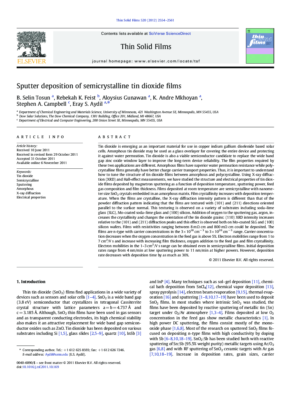
Tin dioxide is emerging as an important material for use in copper indium gallium diselenide based solar cells. Amorphous tin dioxide may be used as a glass overlayer for covering the entire device and protecting it against water permeation. Tin dioxide is also a viable semiconductor candidate to replace the wide band gap zinc oxide window layer to improve the long-term device reliability. The film properties required by these two applications are different. Amorphous films have superior water permeation resistance while polycrystalline films generally have better charge carrier transport properties. Thus, it is important to understand how to tune the structure of tin dioxide films between amorphous and polycrystalline. Using X-ray diffraction (XRD) and Hall-effect measurements, we have studied the structure and electrical properties of tin dioxide films deposited by magnetron sputtering as a function of deposition temperature, sputtering power, feed gas composition and film thickness. Films deposited at room temperature are semicrystalline with nanometer size SnO2 crystals embedded in an amorphous matrix. Film crystallinity increases with deposition temperature. When the films are crystalline, the X-ray diffraction intensity pattern is different than that of the powder diffraction pattern indicating that the films are textured with (101) and (211) directions oriented parallel to the surface normal. This texturing is observed on a variety of substrates including soda-lime glass (SLG), Mo-coated soda-lime glass and (100) silicon. Addition of oxygen to the sputtering gas, argon, increases the crystallinity and changes the orientation of the tin dioxide grains: (110) XRD intensity increases relative to the (101) and (211) diffraction peaks and this effect is observed both on Mo-coated SLG and (100) silicon wafers. Films with resistivities ranging between 8 mΩ cm and 800 mΩ cm could be deposited. The films are n-type with carrier concentrations in the 3 Ã 1018 cmâ 3 to 3 Ã 1020 cmâ 3 range. Carrier concentration decreases when the oxygen concentration in the feed gas is above 5%. Electron mobilities range from 1 to 7 cm2/V s and increase with increasing film thickness, oxygen addition to the feed gas and film crystallinity. Electron mobilities in the 1-3 cm2/V s range can be obtained even in semicrystalline films. Initial deposition rates range from 4 nm/min at low sputtering power to 11 nm/min at higher powers. However, deposition rate decreases with deposition time by as much as 30%.
ناشر
Database: Elsevier - ScienceDirect (ساینس دایرکت)
Journal: Thin Solid Films - Volume 520, Issue 7, 31 January 2012, Pages 2554-2561
Journal: Thin Solid Films - Volume 520, Issue 7, 31 January 2012, Pages 2554-2561
نویسندگان
B. Selin Tosun, Rebekah K. Feist, Aloysius Gunawan, K. Andre Mkhoyan, Stephen A. Campbell, Eray S. Aydil,