| کد مقاله | کد نشریه | سال انتشار | مقاله انگلیسی | نسخه تمام متن |
|---|---|---|---|---|
| 1669605 | 1008885 | 2009 | 4 صفحه PDF | دانلود رایگان |
عنوان انگلیسی مقاله ISI
Residual stress on nanocrystalline silicon thin films deposited under energetic ion bombardment by using internal ICP-CVD
دانلود مقاله + سفارش ترجمه
دانلود مقاله ISI انگلیسی
رایگان برای ایرانیان
کلمات کلیدی
موضوعات مرتبط
مهندسی و علوم پایه
مهندسی مواد
فناوری نانو (نانو تکنولوژی)
پیش نمایش صفحه اول مقاله

چکیده انگلیسی
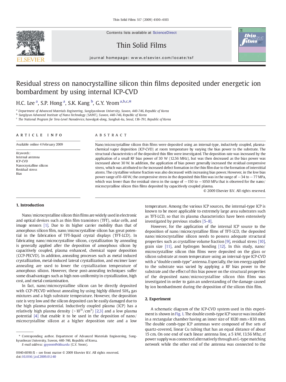
Nano/microcrystalline silicon thin films were deposited using an internal-type, inductively coupled, plasma-chemical vapor deposition (ICP-CVD) at room temperature by varying the bias power to the substrate. The structural characteristics of the deposited thin film were investigated. The deposition rate was increased by the application of a small RF bias power of 30 W (12.56 MHz), but was then decreased as the bias power was increased above 30 W. In addition, the application of bias power generally increased the residual compressive stress, which was attributed to the increased defect formation in the thin film due to the formation of interstitial atoms. The crystalline volume fraction was also decreased with increasing bias power. However, in the low bias power range of 0-60 W, the compressive stress in the deposited thin film was in the range of â 34 to â 77 MPa, which was lower than the residual stress in the range of â 150 to â 1050 MPa that is observed for the nano/microcrystalline silicon thin films deposited by capacitively coupled plasma.
ناشر
Database: Elsevier - ScienceDirect (ساینس دایرکت)
Journal: Thin Solid Films - Volume 517, Issue 14, 29 May 2009, Pages 4100-4103
Journal: Thin Solid Films - Volume 517, Issue 14, 29 May 2009, Pages 4100-4103
نویسندگان
H.C. Lee, S.P. Hong, S.K. Kang, G.Y. Yeom,